LC866548/40/32/28/24A
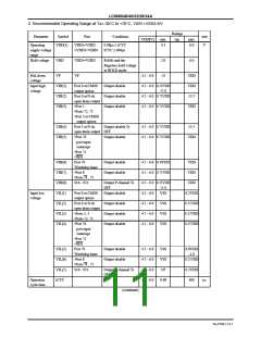
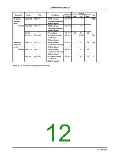
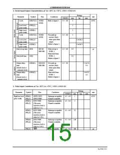
4. Serial Input/Output Characteristics at Ta=-30°C to +70°C, VSS1=VSS2=0V
Ratings
typ.
Parameter
Cycle
Symbol
Pins
Conditions
unit
VDD[V]
4.5 - 6.0
min.
2
max.
tCKCY(1) •SCK0
•SCK1
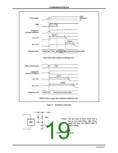
Refer to figure 5.
tCYC
Low Level
tCKL(1)
1
1
2
pulse width
High Level
pulse width
Cycle
tCKH(1)
tCKCY(2) •SCK0
•SCK1
•Use pull-up
4.5 - 6.0
4.5 - 6.0
4.5 - 6.0
resistor (1k
)
Ω
when open drain
output.
Low Level
pulse width
High Level
pulse width
tCKL(2)
1/2tCKCY
1/2tCKCY
•Refer to figure 5.
tCKH(2)
Data set up time tICK
SI0 SI1
•Data set-up to
SCK0, 1.
0.1
0.1
s
µ
SB0 SB1
•Data hold from
SCK0, 1.
Data hold time
tCKI
•Refer to figure 5.
Output delay
time
tCKO(1)
SO0 SO1
SB0 SB1
•Use pull-up
resistor (1kΩ)
when open drain
output.
7/12tCYC
+0.2
(Serial clock is
external clock)
Output delay
time
•Data hold from
SCK0, 1
tCKO(2)
1/3tCYC
+0.2
•Refer to figure 5.
(Serial clock is
internal clock)
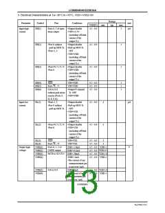
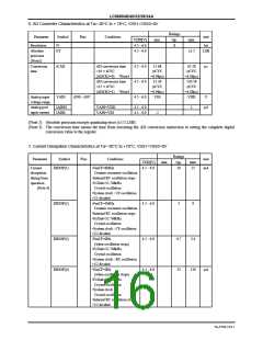
5. Pulse Input Conditions at Ta=-30°C to +70°C, VSS1=VSS2=0V
Ratings
typ.
Parameter
Symbol
Pins
Conditions
unit
VDD[V]
4.5 - 6.0
min.
max.
High/low level tPIH(1)
•INT0, INT1
•INT2/T0IN
INT3/T0IN
•Interrupt acceptable
•Timer0-countable
•Interrupt acceptable
•Timer0-countable
1
tCYC
pulse width
tPIL(1)
tPIH(2)
tPIL(2)
4.5 - 6.0
4.5 - 6.0
4.5 - 6.0
4.5 - 6.0
2
(The noise
rejection clock is
select to 1/1.)
INT3/T0IN
tPIH(3)
tPIL(3)
•Interrupt acceptable
•Timer0-countable
32
(The noise
rejection clock is
select to 1/16.)
INT3/T0IN
tPIH(4)
tPIL(4)
•Interrupt acceptable
•Timer0-countable
128
200
(The noise
rejection clock is
select to 1/64.)
RES
tPIL(5)
Reset acceptable
s
µ
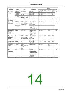
No.6700-15/21

 SANYO [ SANYO SEMICON DEVICE ]