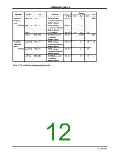
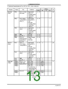
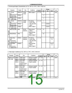
LC866548/40/32/28/24A
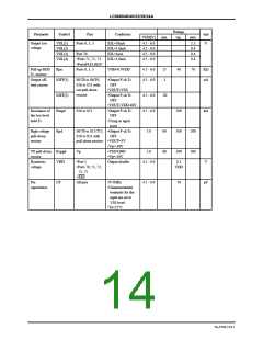
6. AD Converter Characteristics at Ta=-30°C to + 70°C, VSS1=VSS2=0V
Ratings
typ.
Parameter
Symbol
Pins
Conditions
unit
VDD[V]
4.5 - 6.0
4.5 - 6.0
min.
max.
±1.5
Resolution
Absolute
precision
(Note2)
N
8
bit
ET
LSB
Conversion
time
tCAD
AD conversion time
=16 × tCYC
(ADCR2=0) *Note3
AD conversion time
=32 × tCYC
4.5 - 6.0
4.5 - 6.0
4.5 - 6.0
15.68
65.28
µs
(tCYC
(tCYC
=0.98 s)
=4.08 s)
µ
µ
31.36
(tCYC
=0.98µs)
VSS
130.56
(tCYC
=4.08µs)
VDD
(ADCR2=1) *Note3
Analog input
voltage range
Analog port
input current
VAIN
AN0 - AN7
V
IAINH
IAINL
VAIN=VDD
VAIN=VSS
4.5 - 6.0
4.5 - 6.0
1
µA
-1
(Note 2) Absolute precision excepts quantizing error (±1/2 LSB).
(Note 3) The conversion time means the time from executing the AD conversion instruction to setting the complete digital
conversion value to the register.
7. Current Dissipation Characteristics at Ta=-30°C to +70°C, VSS1=VSS2=0V
Ratings
Parameter
Symbol
Pins
Conditions
•FmCF=6MHz
unit
mA
VDD[V]
4.5 - 6.0
min.
typ.
10
max.
25
Current
IDDOP(1)
dissipation
during basic
operation
(Note 4)
Ceramic resonator oscillation
•Internal RC oscillation stops.
•FsXtal=32.768kHz
Crystal oscillation
•System clock : CF oscillation
•1/1 divided
IDDOP(2)
•FmCF=3MHz
4.5 - 6.0
3
9
Ceramic resonator oscillation
•Internal RC oscillation stops.
•FsXtal=32.768kHz
Crystal oscillation
•System clock : CF oscillation
•1/2 divided
IDDOP(3)
IDDOP(4)
•FmCF=0Hz
4.5 - 6.0
0.7
35
3.4
(when oscillation stops)
•FsXtal=32.768kHz
Crystal oscillation
•System clock : RC oscillation
•1/2 divided
•FmCF=0Hz
4.5 - 6.0
130
µA
(when oscillation stops)
•FsXtal=32.768kHz
Crystal oscillation
•System clock :
Crystal oscillation
•Internal RC oscillation stops.
•1/2 divided
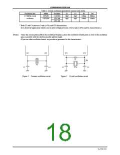
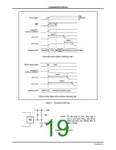
No.6700-16/21

 SANYO [ SANYO SEMICON DEVICE ]