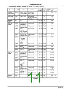
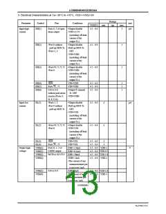
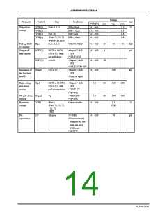
LC866548/40/32/28/24A
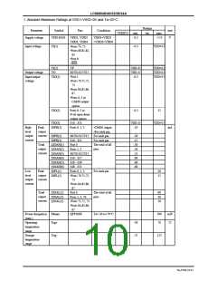
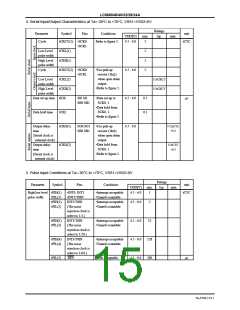
2. Recommended Operating Range at Ta=-30°C to +70°C, VSS1=VSS2=0V
Ratings
typ.
Parameter
Symbol
VDD(1)
Pins
Conditions
unit
V
VDD[V]
min.
4.5
max.
6.0
Operating
supply voltage
range
VDD1=VDD2
=VDD3=VDD4
0.98 s tCYC
µ ≤
tCYC ≤ 400µs
Hold voltage
VHD
VDD1=VDD2
VP
RAMs and the
2.0
-35
6.0
Registers hold voltage
at HOLD mode.
Pull-down
voltage
VP
4.5 - 6.0
VDD
VDD
13.5
Input high
voltage
VIH(1)
VIH(2)
VIH(3)
Port 0 at CMOS
output option
Port 0 at N-ch
open drain output
•Port 1
Output disable
Output disable
Output disable
4.5 - 6.0 0.33VDD
+1.0
4.5 - 6.0 0.75VDD
0.75VDD
4.5 - 6.0
VDD
•Ports 72, 73
•Port 3 at CMOS
output option
Port 3 at N-ch
VIH(4)
VIH(5)
Output disable Tr.
4.5 - 6.0 0.75VDD
4.5 - 6.0 0.75VDD
13.5
open drain output OFF
•Port 70
Output disable
VDD
port input
/interrupt
•Port 71
• RES
VIH(6)
VIH(7)
VIH(8)
VIL(1)
VIL(2)
VIL(3)
VIL(4)
Port 70
Output disable
Output disable
4.5 - 6.0 0.9VDD
4.5 - 6.0 0.75VDD
VDD
VDD
Watchdog timer
•Port 8
•Ports 74 , 75
S16 - S51
Output P-channel Tr.
OFF
4.5 - 6.0 0.33VDD
+1.0
VDD
Input low
voltage
Port 0 at CMOS
output option
Port 0 at N-ch
open drain output
•Ports 1, 3
•Ports 72, 73
•Port 70
Output disable
4.5 - 6.0
4.5 - 6.0
4.5 - 6.0
4.5 - 6.0
VSS
VSS
VSS
VSS
0.2VDD
0.25VDD
0.25VDD
0.25VDD
Output disable
Output disable
Output disable
port input
/interrupt
•Port 71
• RES
VIL(5)
VIL(6)
VIL(7)
tCYC
Port 70
Output disable
Output disable
4.5 - 6.0
4.5 - 6.0
4.5 - 6.0
4.5 - 6.0
VSS
VSS
VP
0.8VDD
-1.0
Watchdog timer
•Port 8
0.25VDD
•Ports 74 , 75
S16 - S51
Output P-channel Tr.
OFF
0.2VDD
400
Operation
cycle time
0.98
µs
(continue)
No.6700-11/21

 SANYO [ SANYO SEMICON DEVICE ]