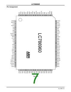
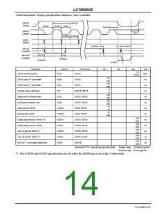
LC786960E
Continued from the previous page.
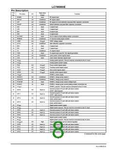
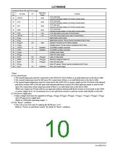
Pin
State when
"Reset"
Pin name
I/O
Function
No.
JTAG reset input
82
JTRSTB
I
I
I
I
Input
Input
Input
Input
(Connect to pll-down resister or 0V level in normal mode.)
JTAG clock input
83
84
85
JTCK
JTDI
(Connect to pll-down resister or 0V level in normal mode.)
JTAG data input
(Connect to pll-down resister or 0V level in normal mode.)
JTAG mode input
JTMS
(Connect to pll-up resister or DV
DD
level in normal mode.)
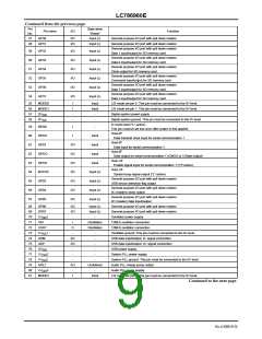
86
87
88
89
90
91
92
93
94
95
96
97
98
99
100
JTDO
O
O
-
Low
JTAG data output (Leave open in normal mode.)
JTAG return clock output (Leave open in normal mode.)
Digital system power supply
JTRTCK
Low
DV
DD
-
DV
SS
-
-
Digital system ground. This pin must be connected to the 0V level.
Capacitor connection pin for internal regulator
Oscillator ground. This pin must be connected to the 0V level.
16.9344MHz oscillator connection
DV 15
DD
AO
-
High
XV
2
-
SS
X16OUT
X16IN
O
I
Oscillation
Oscillation
16.9344MHz oscillator connection
XV
2
-
-
-
Oscillator power supply
DD
LRV
-
Audio LPF power supply
DD
LCHO
LRREF
RCHO
AO
AO
AO
-
LRV /2
DD
Audio Lch data output
LRV /2
DD
Reference voltage for audio LPF
LRV /2
DD
Audio Rch data output
LRV
SS
-
Audio LPF ground. This pin must be connected to the 0V level.
Slice Level Control output
SLCO
AO
Undefined
<Note>
(1) For unused pins:
The unused input pins must be connected to the GND (0V) level if there is no individual note in the above table.
The unused output pins must be left open (No connection) if there is no individual note in the above table.
The unused input/output pins must be connected to the GND (0V) or power supply pin for I/O block with internal
pull down resistor OFF or be left open with internal pull down resistor ON when input pin mode or must be left
open (No connection) when output pin mode if there is no individual note in the above table.
When you connect an I/O pin which is an input pin without internal pull-down resistor at reset mode to the GND
or power supply level, we recommend you to use pull-down resistor or pull-up resistor individually as fail-safe.
(2) For power supply pins:
Same voltage level must be supplied to DV , AV , XV 1, XV 2, VV 1, VV 2, VV 3, UV
DD DD DD DD DD DD DD
DD
and LRV
DD
power supply pins.
(Refer to“Allowable operating ranges”.)
(3) For “Reset” condition:
This LSI is not reset only by making the RESB pin “Low”.
Refer to “Power on and Reset control” for detail of “Reset” condition.
No.A2080-10/24

 SANYO [ SANYO SEMICON DEVICE ]