LC75852E, 75852W
Allowable Operating Ranges at Ta = –40 to +85°C, VSS = 0 V
Parameter
Supply voltage
Symbol
VDD
Conditions
min
4.5
typ
max
6.0
Unit
V
VDD
VIH1
VIH2
VIL
CE, CL, DI, RES
KI1 to KI5
0.8 VDD
0.6 VDD
0
VDD
VDD
V
Input high-level voltage
V
Input low-level voltage
CE, CL, DI, RES, KI1 to KI5
0.2 VDD
V
Recommended external
resistance
ROSC
COSC
OSC
62
kΩ
Recommended external
capacitance
OSC
680
50
pF
Guaranteed oscillator range
Data setup time
Data hold time
fOSC
tds
tdh
tcp
tcs
tch
tøH
tøL
tr
OSC
25
160
160
160
160
160
160
160
100
kHz
ns
ns
ns
ns
ns
ns
ns
ns
ns
µs
µs
µs
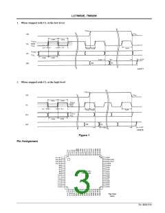
CL, DI: Figure 1
CL, DI: Figure 1
CE wait time
CE, CL: Figure 1
CE setup time
CE, CL: Figure 1
CE hold time
CE, CL: Figure 1
High-level clock pulse width
Low-level clock pulse width
Rise time
CL: Figure 1
CL: Figure 1
CE, CL, DI: Figure 1
CE, CL, DI: Figure 1
DO, RPU = 4.7 kΩ, CL = 10 pF*: Figure 1
DO, RPU = 4.7 kΩ, CL = 10 pF*: Figure 1
Figure 2
160
160
Fall time
tf
DO output delay time
DO rise time
tdc
tdr
1.5
1.5
RES switching time
t2
10
Note: * Since DO is an open-drain output, these values differ depending on the pull-up resistor RPU and the load capacitance CL.
Electrical Characteristics in the Allowable Operating Ranges
Parameter
Symbol
VH
Conditions
CE, CL, DI, RES, KI1 to KI5
min
typ
max
5.0
Unit
V
Hysteresis
0.1 VDD
Input high-level current
Input low-level current
Input floating voltage
Pull-down resistance
Output off leakage current
IIH
CE, CL, DI, RES: VI = 6.0 V
CE, CL, DI, RES: VI = 0 V
KI1 to KI5
µA
µA
V
IIL
–5.0
VIF
0.05 VDD
250
RPD
IOFFH
KI1 to KI5: VDD = 5.0 V
50
100
kΩ
µA
V
DO: VO = 6.0 V
6.0
VOH1
VOH2
VOH3
VOH4
KS1 to KS6: IO = –1 mA
P1 to P4: IO = –1 mA
VDD – 1.0
VDD – 1.0
VDD – 1.0
VDD – 0.6
0.4
V
Output high-level voltage
S1 to S45: IO = –10 µA
V
COM1, COM2: IO = –100 µA
KS1 to KS6: IO = 50 µA
P1 to P4: IO = 1 mA
V
VOL1
VOL2
VOL3
VOL4
VOL5
1.0
3.0
1.0
1.0
0.6
0.5
3.6
2.85
5
V
V
Output low-level voltage
S1 to S45: IO = 10 µA
V
COM1, COM2: IO = 100 µA
DO: IO = 1 mA
V
0.1
3.0
V
V
MID1
MID2
COM1, COM2: VDD = 6.0 V, IO = ±100 µA
COM1, COM2: VDD = 4.5 V, IO = ±100 µA
Sleep mode, Ta = 25°C
VDD = 6.0 V, output open, Ta = 25°C, fOSC = 50 kHz
2.4
V
Output middle-level voltage
Current drain
V
1.65
2.25
V
I
I
DD1
DD2
µA
mA
1.4
2.5
No. 4828-2/16

 SANYO [ SANYO SEMICON DEVICE ]