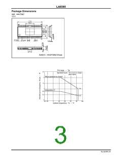
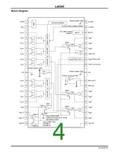
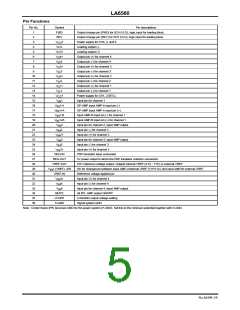
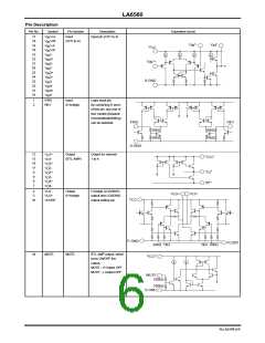
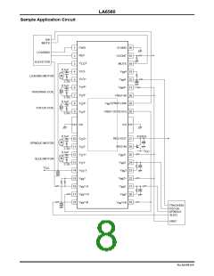
LA6560
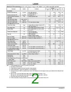
Electrical Characteristics at Ta = 25°C, V 1 = V 2 = 8V, VREF = 2.5V, unless especially specified.
CC CC
Ratings
Parameter
Symbol
Conditions
Unit
mA
min
typ
max
ALL Blocks
No-load current drain ON
I
-ON
BTL-AMP output ON,
30
50
15
CC
LOADING block OFF *1
No-load current drain OFF
Thermal shutdown temperature
VREF AMP
I
-OFF
CC
10
mA
All outputs OFF *1
TSD
150
175
200
°C
Design guarantee value
-10
1
10
-1.5
6.6
mV
V
VREF-AMP offset voltage
VREF Input voltage range
VREF-OUT output current
BTL AMP Block (CH1 to CH4)
Output offset voltage
VREF-OFFSET
VREF-IN
V
V
CC
CH1 input reference voltage
2
5
mA
I-VREF-OUT
V
Voltage difference between outputs for BTL
AMP, each channel. *2
-50
50
mV
OFF
V
Input voltage range for input for OP-AMP.
0
-1.5
mA
V
Input voltage range
Output voltage
IN
CC
V
Each voltage between V + and V - when
5.7
6.2
O
0
0
R
= 8Ω. *3
L
Closed-circuit voltage gain
Slew rate
VG
SR
Input and output gain.
Input OP-AMP:BUFFER
AMP Independent
3.6
2
4
4.4
Times
0.5
V/μs
Multiply 2 between outputs.
VMUTE-ON
VMUTE-OFF
Output ON voltage, each MUTE *4
Output OFF voltage, each MUTE *4
V
V
MUTE ON voltage
0.5
MUTE OFF voltage
Input AMP Block (CH1 to 4)
0
2
V
-1.5
V
mA
μA
mV
V
Input voltage range
V
-OP
CC
IN
Output current (SINK)
SINK-OP
*5
300
-10
2
500
Output current (SOURCE)
Output offset voltage
SOURCE-OP
10
V
-OP
OFF
CH1 input AMP(B), external REF select *6
CH1 input AMP(A), internal VREF select *6
CH1 input changeover voltage 1
CH1 input changeover voltage 2
Loading Block (CH5, H bridge)
Output voltage
VSW-OP1
VSW-OP2
0.5
V
V
-LOAD
At forward and reverse rotation,
5.7
6.5
V
O
R
= 8Ω, VCONT=V
*3
L
CC
0.3
1
V
V
V
Break output saturation voltage
Input low level
V
-BREAK
Output voltage at braking *7
CE
V
-L
IN
Input high level
V -H
IN
2
Power Supply Block (PNP transistor : 2SB632K-use)
5V supply voltage
REG-IN SINK current
Line regulation
V
I
= 200mA
O
4.8
5
5.0
10
10
10
5.2
V
OUT
REG-IN-SINK
ΔV LN
Base current of external PNP *8
6V ≤ V ≤ 12V, I = 200mA
mA
mV
mV
100
100
O
CC
O
Load regulation
ΔV LD
O
5mA ≤ I ≤ 200mA
O
Note *1 : Current dissipation that is a sum of V 1 and V 2 at no load.
CC CC
*2 : Input AMP is a BUFFER AMP.
*3 : Voltage difference between both ends of load (8Ω). Output saturated.
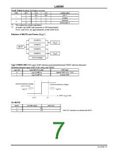
*4 : Output ON with MUTE : [H] and OFF with MUTE : [L] (HI impedance).
*5 : The source of input OP-AMP is a constant current. As the 11kΩ resistance to the next stage is a load, pay due attention when setting the input
OP-AMP gain.
*6 : With V 1-SW : [L], the input AMP selects AMP-A while VREF selects internal VREF (≈ 2.5V).
IN
With V 1-SW : [H], the input AMP selects AMP-B while VREF selects external VREF (≈ VREF-IN).
IN
*7 : Short (GND) brake used. SINK side output ON.
*8 : 5VREG incorporates a drooping protection circuit and operated when the base current is 10mA (TYP).
No.A0599-2/9

 SANYO [ SANYO SEMICON DEVICE ]