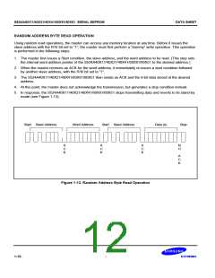
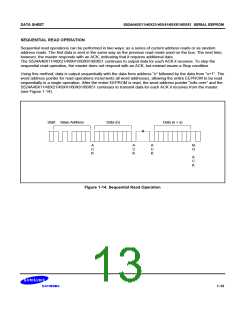
DATA SHEET
S524A40X11/40X21/40X41/60X81/60X51 SERIAL EEPROM
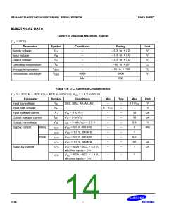
Table 1-4. D.C. Electrical Characteristics (Continued)
°
°
°
°
(TA = – 25 C to + 70 C (C), – 40 C to + 85 C (I), VCC = 1.8 V to 5.5 V)
Parameter
Symbol
Conditions
Min
Typ
Max
Unit
CIN
–
–
10
pF
°
Input capacitance
25 C, 1MHz,
VCC = 5 V, VIN = 0 V,
A0, A1, A2, SCL and WP pin
CI/O
–
–
10
°
Input/output capacitance
25 C, 1MHz,
VCC = 5 V, VI/O = 0 V,
SDA pin
Table 1-5. A.C. Electrical Characteristics
°
°
°
°
(TA = – 25 C to + 70 C (C), – 40 C to + 85 C (I), VCC = 1.8 V to 5.5 V)
Parameter
Symbol Conditions
VCC = 1.8 to 5.5 V
(Standard Mode)
VCC = 2.5 to 5.5 V
(Fast Mode)
Unit
Min
Max
Min
Max
FCLK
tHIGH
tLOW
External clock frequency
Clock high time
–
0
100
0
400
kHz
–
4
4.7
–
–
–
0.6
1.3
–
–
–
ms
Clock low time
–
tR
Rising time
SDA, SCL
1
0.3
0.3
–
tF
Falling time
SDA, SCL
–
0.3
–
–
tHD:STA
tSU:STA
tHD:DAT
tSU:DAT
tSU:STO
tBUF
Start condition hold time
Start condition setup time
Data input hold time
Data input setup time
Stop condition setup time
Bus free time
–
–
–
–
–
4
0.6
0.6
0
4.7
0
–
–
–
–
0.25
4
–
0.1
0.6
1.3
–
–
–
Before new
4.7
–
–
transmission
tAA
Data output valid from
clock low (note)
–
0.3
3.5
–
0.9
tSP
Noise spike width
Write cycle time
–
–
–
–
100
5
–
–
50
5
ns
tWR
ms
NOTE: When acting as a transmitter, the S524A40X11/40X21/40X41/60X81/60X51 must provide an internal minimum
delay time to bridge the undefined period (minimum 300 ns) of the falling edge of SCL. This is required to avoid
unintended generation of a start or stop condition.
1-15

 SAMSUNG [ SAMSUNG ]