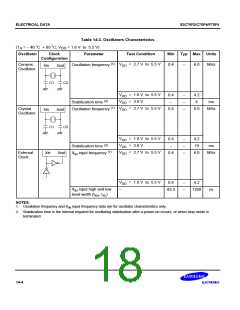
S3C70F2/C70F4/P70F4
ELECTRICAL DATA
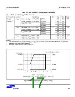
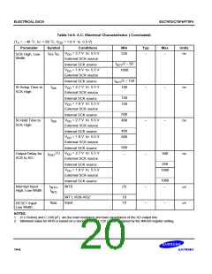
Table 14-7. RAM Data Retention Supply Voltage in Stop Mode
°
°
(TA = – 40 C to + 85 C)
Parameter
Symbol
Conditions
Min
1.8
–
Typ
–
Max
5.5
10
Unit
VDDDR
Data retention supply voltage
Data retention supply current
–
V
IDDDR
VDDDR = 1.8 V
0.1
mA
tSREL
tWAIT
Release signal set time
–
0
–
–
–
–
ms
217 / fx
Oscillator stabilization wait
time (1)
ms
Released by RESET
(2)
Released by interrupt
–
–
ms
NOTES:
1. During oscillator stabilization wait time, all CPU operations must be stopped to avoid instability during oscillator start-
up.
2. Use the basic timer mode register (BMOD) interval timer to delay execution of CPU instructions during the wait time.
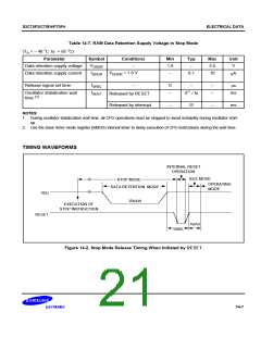
TIMING WAVEFORMS
INTERNAL RESET
OPERATION
IDLE MODE
OPERATING
MODE
STOP MODE
DATA RETENTION MODE
VDD
VDDDR
EXECUTION OF
STOP INSTRUCTION
RESET
tWAIT
tSREL
Figure 14-2. Stop Mode Release Timing When Initiated by RESET
14-7

 SAMSUNG [ SAMSUNG ]