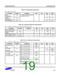
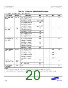
ELECTRICAL DATA
S3C70F2/C70F4/P70F4
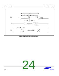
Table 14-6. A.C. Electrical Characteristics ( Concluded)
°
°
(TA = – 40 C to + 85 C, VDD = 1.8 V to 5.5 V)
Parameter
Symbol
Conditions
Min
Typ
Max
Units
tKH, tKL VDD = 2.7 V to 5.5 V
335
–
–
ns
SCK High, Low
Width
External SCK source
tKCY/2 – 50
1600
Internal SCK source
VDD = 1.8 V to 5.5 V
External SCK source
tKCY/2 – 150
100
Internal SCK source
tSIK
VDD = 2.7 V to 5.5 V
SI Setup Time to
–
–
–
–
ns
ns
ns
SCK High
External SCK source
150
150
Internal SCK source
VDD = 1.8 V to 5.5 V
External SCK source
500
400
Internal SCK source
VDD = 2.7 V to 5.5 V
External SCK source
tKSI
SI Hold Time to
–
SCK High
400
600
Internal SCK source
VDD = 1.8 V to 5.5 V
External SCK source
500
–
Internal SCK source
VDD = 2.7 V to 5.5 V
External SCK source
(1)
Output Delay for
300
tKSO
SCK to SO
250
Internal SCK source
VDD = 1.8 V to 5.5 V
External SCK source
1000
1000
–
Internal SCK source
(2)
tINTH
tINTL
,
Interrupt Input
High, Low Width
INT0
–
–
ms
ms
INT1, KS0–KS2
Input
10
10
t
–
RSL
RESET Input
Low Width
NOTES:
1. R (1 Kohm) and C (100 pF) are the load resistance and load capacitance of the SO output line.
2. Minimum value for INT0 is based on a clock of 2tCY or 128 / fx as assigned by the IMOD0 register setting.
14-6

 SAMSUNG [ SAMSUNG ]