S3C70F2/C70F4/P70F4
ELECTRICAL DATA
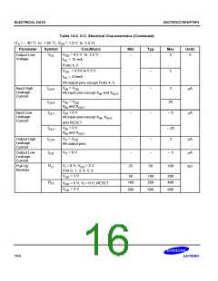
Table 14-2. D.C. Electrical Characteristics (Concluded)
°
°
(TA = – 40 C to + 85 C, VDD = 1.8 V to 5.5 V)
Parameter Symbol
Conditions
Min
Typ
Max Units
mA
8.0
IDD1
IDD2
IDD3
Supply
6.0MHz
–
3.0
Run mode; VDD = 5.0 V ± 10%
Current (1)
Crystal oscillator; C1=C2=22pF
4.19MHz
6.0MHz
2.0
1.3
5.5
4.0
VDD = 3 V ± 10%
4.19MHz
6.0MHz
1.0
0.8
3.0
mA
2.5
–
–
Idle mode; VDD = 5.0 V ± 10%
Crystal oscillator; C1=C2=22pF
4.19MHz
6.0MHz
0.6
0.6
1.8
1.5
VDD = 3 V ± 10%
4.19MHz
0.4
0.5
1.0
3.0
2.0
Stop mode; VDD = 5.0 V ± 10%
Stop mode; VDD = 3.0 V ± 10%
mA
0.3
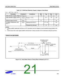
NOTES:
1. D.C. electrical values for Supply current (I
to I
) do not include current drawn through internal pull-up resistor,
DD3
DD1
output port drive currents and comparator.
2. The supply current assumes a CPU clock of fx/4.
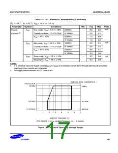
Main Osc. Freq. ( Divided by 4 )
6 MHz
CPU CLOCK
1.5 MHz
1.05 MHz
4.2 MHz
400 kHz
15.625 kHz
2.7
1
2
3
4
5
6
7
SUPPLY VOLTAGE (V)
CPU CLOCK = 1/n x oscillator frequency (n = 4, 8 or 64)
Figure 14-1. Standard Operating Voltage Range
14-3

 SAMSUNG [ SAMSUNG ]