S3C70F2/C70F4/P70F4
PRODUCT OVERVIEW
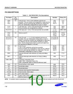
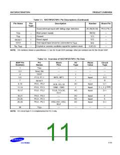
Table 1-1. S3C70F2/C70F4 Pin Descriptions (Continued)
Description
Pin Name
Pin
Type
Number
26-28(28-30)
Share Pin
Quasi-interrupt input with falling edge detection
P6.0–P6.2
V
—
—
I
Main power supply
Ground
30(32)
1(1)
—
—
—
—
—
DD
V
SS
Reset signal
7(7)
RESET
Test signal input (must be connected to V
)
SS
TEST
I
4(4)
X , X
in out
—
Crystal or ceramic oscillator signal for system clock
3,2(3,2)
NOTE: Pin numbers shown in parentheses '( )' are for 32-pin SOP package; other pin numbers are for the 30-pin SDIP.
Table 1-2. Overview of S3C70F2/C70F4 Pin Data
SDIP Pin
Numbers
Pin
Names
Share
Pins
I/O
Type
Reset
Value
Circuit
Type
V
1
2,3
4
¾
¾
¾
I
¾
¾
¾
¾
SS
Xout, Xin
TEST
¾
¾
INT0, INT1
¾
¾
¾
5,6
7
P1.0, P1.1
I
Input
¾
A-3
B
I
RESET
8-10
11-14
15-17
P0.0 - P0.2
I/O
I
Input
Input
Input
D-1
SCK, SO, SI
F-1, F-2 (note)
D-1
P2.0 - P2.3
P3.0 - P3.2
CIN0 - CIN3
TCL0, TCLO0,
CLO
I/O
18-21
22-25
26-29
P4.0 - P4.3
P5.0 - P5.3
P6.0 - P6.3
I/O
I/O
I/O
Input
Input
Input
E
E
¾
¾
KS0, KS1, KS2,
BUZ
D-1
V
DD
30
¾
¾
¾
¾
NOTE: I/O circuit type F-2 is implemented for P2.3 only.
1-11

 SAMSUNG [ SAMSUNG ]