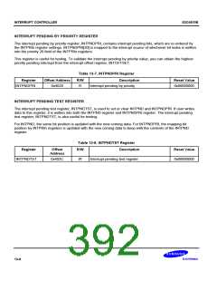
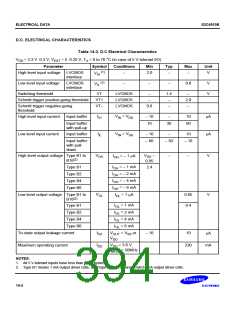
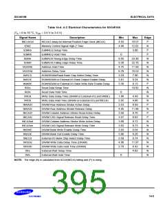
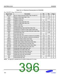
ELECTRICAL DATA
S3C4510B
Table 14-5. A.C Electrical Characteristics for S3C4510B
°
(TA = 0 to 70 C, VDD = 3.0 V to 3.6 V)
Signal Name
Description
Min
4.07
5.08
Max
9.37
Edge
P
tMCLKOd
tEMZ
MCLKO delay for Internal Positive Edge Clock(MCLK)
Memory Control Signal High-Z Time
ExtMREQ Setup Time
11.76
6.31
N
P
tEMRs
tEMRh
tEMAr
ExtMREQ Hold Time
0
P
ExtMACK Rising Edge Delay Time
12.19
9.33
5.16
6.13
3.96
3.82
4.70
28.54
21.87
12.08
14.35
9.29
N
N
N
N
N
N
P
tEMAf
ExtMACK Falling Edge Delay Time
tADDRh
tADDRd
tNRCS
tNROE
tNWBE
tRDs
Address Hold Time
Address Delay Time
ROM/SRAM/Flash Bank Chip Select Delay Time
ROM/SRAM or External I/O Bank Output Enable Delay
ROM/SRAM or External I/O Bank Write Byte Enable Delay
Read Data Setup Time
8.96
11.13
12.46
N
N
N
N
P
tRDh
Read Data Hold Time
0
tWDd
Write Data Delay Time (SRAM or External I/O) (ref:nWBE)
Write Data Hold Time (SRAM or External I/O) (ref:MCLK)
DRAM Row Address Strobe Active Delay
DRAM Row Address Strobe Release Delay
DRAM Column Address Strobe Read Active Delay
DRAM CAS Signal Release Read Delay Time
DRAM Column Address Strobe Write Active Delay
DRAM CAS Signal Release Write Delay Time
DRAM Bank Write Enable Delay Time
DRAM Bank Out Enable Delay Time
External I/O Bank Chip Select Delay Time
DRAM Write Data Delay Time (DRAM)
DRAM Write Data Hold Time (DRAM)
External Wait Setup Time
2.50
1.94
3.84
5.70
3.77
4.23
3.78
4.27
4.81
4.15
4.12
7.00
3.27
5.65
4.45
9.00
13.31
8.84
9.88
8.86
9.99
11.25
9.71
9.63
16.32
7.58
4.46
tWDh
tNRASf
tNRASr
tNCASf
tNCASr
tNCASwf
tNCASwr
tNDWE
tNDOE
tNECS
tWDDd
tWDDh
tWs
N
P
P
N
N
N
N
N
N
N
N
N
tWh
External Wait Hold Time
0
NOTE: The edge (N) is calculated from SCLK(MCLK) falling and (P) is rising.
14-4

 SAMSUNG [ SAMSUNG ]