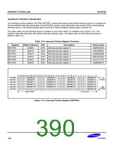
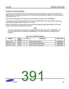
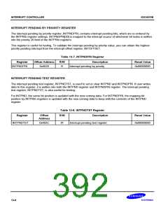
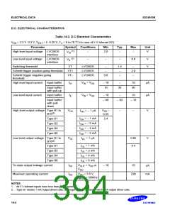
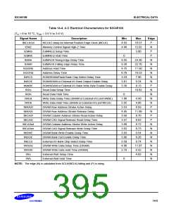
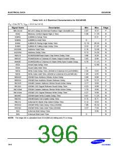
ELECTRICAL DATA
S3C4510B
D.C. ELECTRICAL CHARACTERISTICS
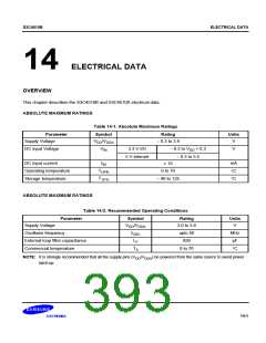
Table 14-3. D.C Electrical Characteristics
°
VDD = 3.3 V 0.3 V, VEXT = 5 0.25 V, TA = 0 to 70 C (in case of 5 V-tolerant I/O)
Parameter
Symbol
Conditions
Min
Typ
Max
Unit
(1)
High level input voltage LVCMOS
interface
–
2.0
–
–
V
VIH
(1)
Low level input voltage
LVCMOS
interface
–
–
–
0.8
V
V
VIL
Switching threshold
VT
LVCMOS
LVCMOS
LVCMOS
–
–
1.4
–
–
2.0
–
Schmitt trigger positive-going threshold
VT+
VT–
Schmitt trigger negative-going
threshold
0.8
–
IIH
VIN = VDD
High level input current
Low level input current
Input buffer
– 10
10
–
10
60
mA
mA
Input buffer
with pull-up
30
IIL
VIN = VSS
Input buffer
– 10
– 60
–
10
Input buffer
with pull-
down
– 30
– 10
VOH
VDD
–
High level output voltage Type B1 to
B16(2)
–
–
V
IOH = – 1 mA
0.05
IOH = – 1 mA
IOH = – 2 mA
IOH = – 4 mA
IOH = – 6 mA
IOL = 1 mA
Type B1
Type B2
Type B4
Type B6
2.4
VOL
Low level output voltage Type B1 to
B16(2)
0.05
0.4
V
IOL = 1 mA
IOL = 2 mA
IOL = 4 mA
IOL = 6 mA
Type B1
Type B2
Type B4
Type B6
IOZ
VOUT = VSS or
VDD
Tri-state output leakage current
– 10
10
mA
IDD
VDD = 3.6 V,
Maximum operating current
230
mA
fMCLK = 50MHz
NOTES:
1. All 5 V-tolerant inputs have less than 0.2 V hysterics.
2. Type B1 means 1 mA output driver cells, and Type B6/B24 means 6 mA/24 mA output driver cells.
14-2

 SAMSUNG [ SAMSUNG ]