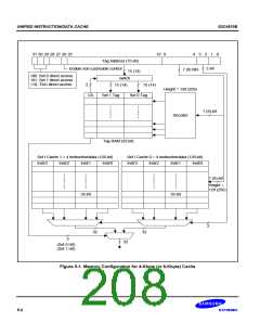
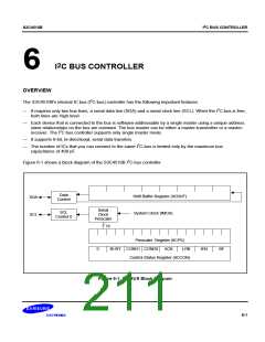
UNIFIED INSTRUCTION/DATA CACHE
CACHE DISABLE/ENABLE
S3C4510B
To disable the cache disable entirely following a system reset, you must set SYSCFG[1] to "0". By setting the
cache mode bits, SYSCFG[5:4], you can specify a cache size of 0, 4, or 8K bytes. If you do not need the entire 8-
Kbyte area for cache, you can use the remaining area as normal internal SRAM. The start address of the internal
SRAM area is defined by writing an appropriate value to SYSCFG[15:6].
CACHE FLUSH OPERATION
To flush cache lines, you must write a zero to Tag memory bits 31 and 30, respectively.
The 4-Kbyte set 0 RAM area, 4-Kbyte set 1 RAM area, and the 1-Kbyte Tag RAM area (total 256 words) can be
accessed from locations 0x10000000H, 0x10800000H, and 0x11000000H, respectively. You can do this
independently of the current cache mode bit and cache enable bit settings.
Tag RAM is normally cleared by hardware following a power-on reset. However, if you change the cache or
memory bank configuration when the cache is being enabled, you will have to clear the Tag RAM area using
application software.
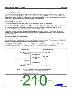
NON-CACHEABLE AREA CONTROL BIT
Although the cache affects the entire system memory, it is sometimes necessary to define non-cacheable areas
when the consistency of data stored in memory and the cache must be ensured. To support this, the S3C4510B
provides a non-cacheable area control bit in the address field, ADDR[26].
If ADDR[26] in the ROM/SRAM, flash memory, DRAM, or external I/O bank's access address is "0", then the
accessed data is cacheable. If the ADDR[26] value is "1", the accessed data is non-cacheable.
Cacheable Area
Non-cacheable Area
000_0000
400_0000
000_0000
Cacheable Area
000_FFFF
401_0000
401_FFFF
Non-cacheable
Area
16 M word
002_0000
3FF_FFFF
Cacheable Area
7FF_FFFF
3FF_FFFF
NOTE:
The non-cacheable area has the same space in memory
as the cacheable area. To access the non-cacheable
area, you can change the address of the space in memory
using non-cacheable control bit.
Figure 5-3. Non-Cacheable Area Control
NOTE
A SWAP command must be used within a non-cacheable area.
5-4

 SAMSUNG [ SAMSUNG ]