KMM372F80(8)3BK/BS
DRAM MODULE
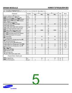
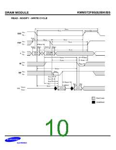
NOTES
An initial pause of 200us is required after power-up followed
by any 8 RAS-only or CAS-before-RAS refresh cycles before
proper device operation is achieved.
1.
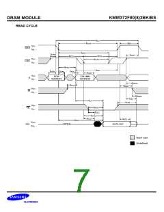
Either tRCH or tRRH must be satisfied for a read cycle.
8.
9.
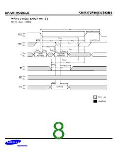
These parameters are referenced to the CAS leading edge in
early write cycles.
2. Input voltage levels are Vih/Vil. VIH(min) and VIL(max) are ref-
erence levels for measuring timing of input signals. Transi-
tion times are measured between VIH(min) and VIL(max) and
are assumed to be 5ns for all inputs.
Operation within the tRAD(max) limit insures that tRAC(max)
can be met. tRAD(max) is specified as reference point only. If
tRAD is greater than the specified tRAD(max) limit, then
access time is controlled by tAA.
10.
11.
3.
Measured with a load equivalent to 1 TTL loads and 100pF.
If RAS goes high before CAS high going, the open circuit
condition of the output is achieved by CAS high going. If CAS
goes high before RAS high going , the open circuit condition
of the output is achieved by RAS going.
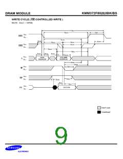
4. Operation within the tRCD(max) limit insures that tRAC(max)
can be met. tRCD(max) is specified as a reference point only.
If tRCD is greater than the specified tRCD(max) limit, then
access time is controlled exclusively by tCAC.
12.
13.
tASC ³ 6ns.
5.
6.
Assumes tha tRCD³ tRCD(max).
The timing skew from the DRAM to the DIMM resulted from
the addition of buffers.
This parameter defines the time at which the output achieves
the open circuit condition and is not referenced to VOH or
VOL.
7. tWCS, tRWD, tCWD, tAWD and tCPWD are not restrictive operat-
ing parameter. They are included in the data sheet as electri-
cal characteristics only. If tWCS³ tWCS(min) the cycle is an
early write cycle and the data out pin will remain high imped-
ance for the duration of the cycle. If tRWD³ tRWD(min),
tCWD³ tCWD(min), tAWD³ tAWD(min) and tCPWD³ tCPWD(min).
The cycle is a read-modify-write cycle and the data out will
contain data read from the selected cell. If neither of the
above sets of conditions is satisfied, the condition of data
out(at access time) is indeterminate.

 SAMSUNG [ SAMSUNG ]