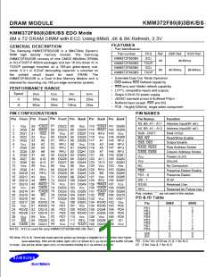
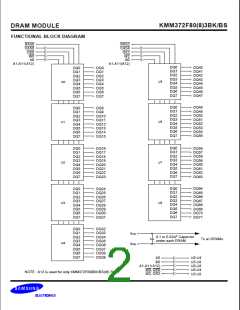
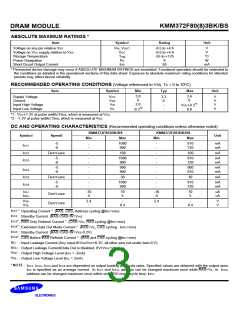
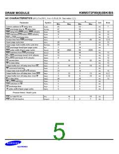
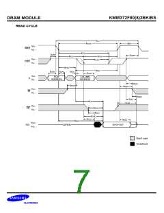
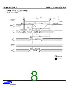
KMM372F80(8)3BK/BS
DRAM MODULE
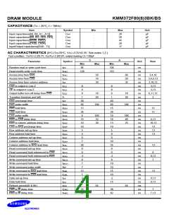
AC CHARACTERISTICS (0°C£TA£70°C, VCC=3.3V±0.3V. See notes 1,2.)
-5
-6
Parameter
Symbol
Unit
Note
Min
45
47
10
8
Max
Min
53
58
10
8
Max
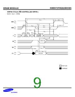
Column address to W delay time
CAS precharge time to W delay time
CAS setup time(CAS-before-RAS refresh)
CAS hold time(CAS-before-RAS refresh)
RAS to CAS precharge time
ns
ns
ns
ns
ns
ns
ns
ns
ns
ns
ns
ns
ns
ns
ns
ns
ns
ns
ns
ns
ns
ns
ns
ns
ns
7
tAWD
tCPWD
tCSR
tCHR
tRPC
tCPA
13
13
3
3
13
Access time from CAS precharge
Hyper page cycle time
33
40
3,13
12
20
70
7
25
77
10
60
40
15
8
tHPC
tHPRWC
tCP
Hyper page read-modify-write cycle time
CAS precharge time(Hyper page cycle)
RAS pulse width (Hyper page cycle)
RAS hold time from CAS precharge
W to RAS precharge time(C-B-R refresh)
W to RAS hold time(C-B-R refresh)
OE access time
12
50
35
15
8
200K
200K
tRASP
tRHCP
tWRP
tWRH
tOEA
tOED
tOEZ
13
13
13
13
13
13
18
18
20
18
OE to data delay
15
8
18
8
Output buffer turn off delay time from OE
OE command hold time
5
5
tOEH
tDOH
tREZ
Output data hold time(C-B-R refresh)
Output buffer turn off delay time from RAS
Output buffer turn off delay time from W
W to data delay
10
3
10
3
13
6,11
6,13
13
13
18
13
18
8
8
tWEZ
tWED
tOCH
tCHO
tOEP
tWPE
20
5
20
5
OE to CAS hold time
CAS hold time to OE
5
5
OE precharge time
5
5
W pulse width (Hyper page cycle)
5
5
Present Detect Read Cycle
PDE to Valid PD bit
10
7
10
7
ns
ns
tPD
PDE to PD bit Inactive
2
2
tPDOFF

 SAMSUNG [ SAMSUNG ]