KMM372F80(8)3BK/BS
DRAM MODULE
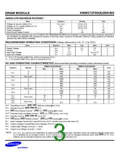
ABSOLUTE MAXIMUM RATINGS *
Item
Symbol
Rating
Unit
Voltage on any pin relative VSS
Voltage on VCC supply relative to VSS
Storage Temperature
VIN, VOUT
VCC
-0.5 to +4.6
-0.5 to +4.6
-55 to +125
9
V
V
°C
W
Tstg
PD
Power Dissipation
Short Circuit Output Current
IOS
50
mA
* Permanent device damage may occur if ABSOLUTE MAXIMUM RATINGS are exceeded. Functional operation should be restricted to
the conditions as detailed in the operational sections of this data sheet. Exposure to absolute maximum rating conditions for intended
periods may affect device reliability.
RECOMMENDED OPERATING CONDITIONS (Voltage referenced to VSS, TA = 0 to 70°C)
Item
Symbol
Min
Typ
Max
Unit
3.0
0
2.0
3.6
0
Supply Voltage
Ground
Input High Voltage
Input Low Voltage
VCC
VSS
VIH
VIL
3.3
0
-
V
V
V
V
*1
VCC+0.3
0.8
*2
-
-0.3
*1 : VCC+1.3V at pulse width£15ns, which is measured at VCC.
*2 : -1.3V at pulse width£15ns, which is measured at VSS.
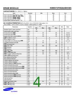
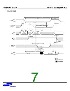
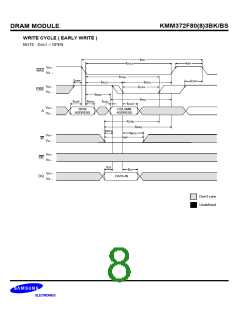
DC AND OPERATING CHARACTERISTICS (Recommended operating conditions unless otherwise noted)
KMM372F803BK/BS
KMM372F883BK/BS
Symbol
Speedl
Unit
Min
Max
Min
Max
-5
-6
1080
990
-
-
810
720
mA
mA
-
--
ICC1
ICC2
ICC3
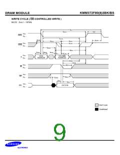
Don¢t care
-
100
-
100
mA
-5
-6
-
-
1080
990
-
-
810
720
mA
mA
-5
-6
-
-
990
900
-
-
900
810
mA
mA
ICC4
ICC5
ICC6
Don¢t care
-
30
-
30
mA
-5
-6
-
-
1080
990
-
-
810
720
mA
mA
II(L)
IO(L)
-10
-5
10
5
-10
-5
10
5
uA
uA
Don¢t care
Don¢t care
VOH
VOL
2.4
-
-
2.4
-
-
V
V
0.4
0.4
ICC1*
ICC2
ICC3*
ICC4*
ICC5
ICC6*
I(IL)
: Operating Current * (RAS, CAS, Address cycling @tRC=min)
: Standby Current (RAS=CAS=W=VIH)
: RAS Only Refresh Current * (CAS=VIH, RAS cycling @tRC=min)
: Extended Data Out Mode Current * (RAS=VIL, CAS cycling : tHPC=min)
: Standby Current (RAS=CAS=W=Vcc-0.2V)
: CAS-Before-RAS Refresh Current * (RAS and CAS cycling @tRC=min)
: Input Leakage Current (Any input 0£VIN£Vcc+0.3V, all other pins not under test=0 V)
: Output Leakage Current(Data Out is disabled, 0V£VOUT£Vcc)
: Output High Voltage Level (IOH = -2mA)
I(OL)
VOH
VOL
: Output Low Voltage Level (IOL = 2mA)
* NOTE :
ICC1, ICC3, ICC4 and ICC6 are dependent on output loading and cycle rates. Specified values are obtained with the output open.
ICC is specified as an average current. In ICC1 and ICC3, address can be changed maximum once while RAS=VIL. In ICC4,
address can be changed maximum once within one EDO mode cycle time, tHPC.

 SAMSUNG [ SAMSUNG ]