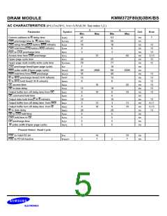
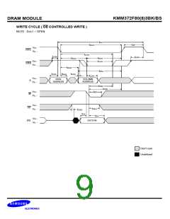
KMM372F80(8)3BK/BS
DRAM MODULE
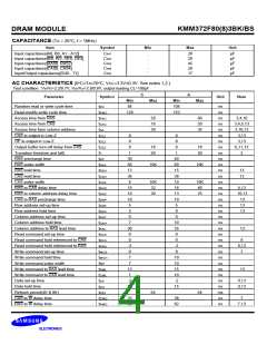
CAPACITANCE (TA = 25°C, f = 1MHz)
Item
Symbol
Min
Max
Unit
Input capacitance[A0, B0, A1 - A12]
Input capacitance[W0, W2, OE0, OE2]
Input capacitance[RAS0, RAS2]
Input capacitance[CAS0, CAS4]
Input/Output capacitance[DQ0 - 71]
CIN1
CIN2
CIN3
CIN4
CDQ
20
20
45
20
17
pF
pF
pF
pF
pF
-
-
-
-
-
AC CHARACTERISTICS (0°C£TA£70°C, VCC=3.3V±0.3V. See notes 1,2.)
Test condition : Vih/Vil=2.2/0.7V, Voh/Vol=2.0/0.8V, output loading CL=100pF
-5
-6
Parameter
Symbol
Unit
Note
Min
84
Max
Min
104
153
Max
Random read or write cycle time
Read-modify-write cycle time
Access time from RAS
ns
ns
ns
ns
ns
ns
ns
ns
ns
ns
ns
ns
ns
ns
ns
ns
ns
ns
ns
ns
ns
ns
ns
ns
ns
ns
ns
ns
ns
ns
ns
ns
ms
ns
ns
tRC
128
tRWC
tRAC
tCAC
tAA
50
18
30
60
20
35
3,4,10
Access time from CAS
3,4,5,13
3,10,13
3,13
Access time from column address
CAS to output in Low-Z
8
8
8
8
tCLZ
tOLZ
tCEZ
tT
OE to output in Low-Z
3,13
Output buffer turn-off delay from CAS
Transition time(rise and fall)
RAS precharge time
8
18
50
8
18
50
6,11,13
2
1
1
30
50
13
36
8
40
60
15
38
10
18
13
10
5
tRP
RAS pulse width
10K
10K
tRAS
tRSH
tCSH
tCAS
tRCD
tRAD
tCRP
tASR
tRAH
tASC
tCAH
tRAL
tRCS
tRCH
tRRH
tWCS
tWCH
tWP
RAS hold time
13
13
CAS hold time
CAS pulse width
10K
32
10K
40
RAS to CAS delay time
15
10
10
5
4,13
10,13
13
RAS to column address delay time
CAS to RAS precharge time
Row address set-up time
Row address hold time
20
25
13
5
8
13
Column address set-up time
Column address hold time
Column address to RAS lead time
Read command set-up time
Read command hold referenced to CAS
Read command hold referenced to RAS
Write command set-up time
Write command hold time
Write command pulse width
Write command to RAS lead time
Write command to CAS lead time
Data set-up time
0
0
7
10
35
0
30
0
13
0
0
8
8,13
7
-2
0
-2
0
7
10
10
15
10
-2
15
7
13
7
13
tRWL
tCWL
tDS
-2
13
9,13
9,13
Data hold time
tDH
Refresh period(4K & 8K)
CAS to W delay time
64
64
tREF
tCWD
tRWD
33
68
38
82
7
RAS to W delay time
7,13

 SAMSUNG [ SAMSUNG ]