OneNAND512Mb(KFG1216U2B-xIB6)
FLASH MEMORY
3.11.5 OTP and 1st Block OTP Lock Operation
OTP and 1st Block can be locked simultaneously, for locking bit lies in the same word of OTP area.
1st Block OTP can be accessed just as any other NAND Flash Array Blocks before it is locked, however, once 1st Block is locked to
be OTP, 1st Block OTP cannot be erased or programmed. Also, OTP area can only be programmed once without erase capability, it
can be locked when the device starts up to prevent any changes from being made.
Locking the OTP and 1st Block OTP
Programming to the OTP area and 1st Block OTP area can be prevented by locking the OTP area. Locking the OTP area is
accomplished by programming XXF0h to 8th word of sector0 in page0 spare area in the OTP block.
At device power-up, this word location is checked and if XXF0h is found, the OTPL and OTPBL bit of the Controller Status Register is
set to "1", indicating the OTP and 1st Block is locked. When the Program Operation finds that the status of the OTP and 1st Block is
locked, the device updates the Error Bit of the Controller Status Register as "1" (fail).
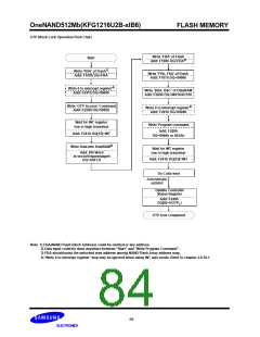
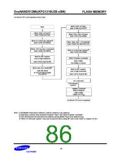
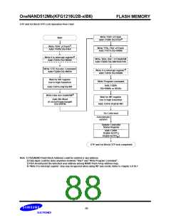
OTP and 1st Block OTP simultaneous Lock Operation Steps
•
•
Issue the OTP Access Command
Fill data to be programmed into DataRAM (data can be input at anytime between the "Start" and
"Write Program" commands)
•
•
•
•
Write 'XXF0h' data into the 8th word of sector0 in page0 spare area of the DataRAM.
Issue a Flash Block Address (FBA) which is unlocked area address of NAND Flash Array address map.
Issue a Program command to program the data from the DataRAM into the OTP
When the 1st Block OTP lock is complete, do a Cold Reset to exit the OTP Access mode
and update 1st Block OTP lock bit[5] and OTP lock bit[6].
• 1st Block OTP lock bit[5] and OTP lock bit[6] of the Controller Status Register will be set to "1" and
the OTP and 1st Block will be locked.
Even though the OTP area can only be programmed once without erase capability, it can be locked when the device starts up to pre-
vent any changes from being made.
Unlike other remaining main area of the NAND Flash Array memory, once the OTP block and the 1st block OTP are locked, it
cannot be unlocked.
87

 SAMSUNG [ SAMSUNG ]