K9W4G08U1M
K9K2G08Q0M
K9K2G08U0M
K9W4G16U1M
K9K2G16Q0M
K9K2G16U0M
FLASH MEMORY
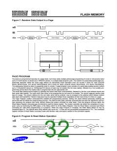
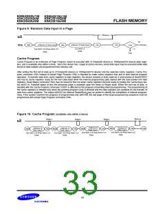
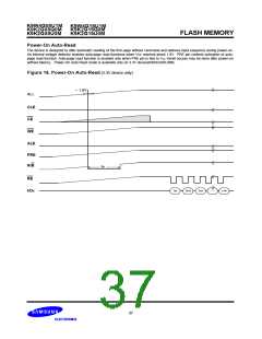
Figure 9. Random Data Input In a Page
tPROG
R/B
"0"
Pass
80h
Address & Data Input
Address & Data Input
I/O0
Fail
85h
10h
70h
I/Ox
Col Add1,2
Data
Col Add1,2 & Row Add1,2,3
Data
"1"
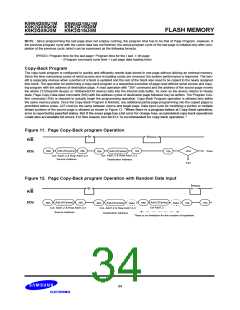
Cache Program
Cache Program is an extension of Page Program, which is executed with 2112byte(X8 device) or 1056word(X16 device) data regis-
ters, and is available only within a block. Since the device has 1 page of cache memory, serial data input may be executed while data
stored in data register are programmed into memory cell.
After writing the first set of data up to 2112byte(X8 device) or 1056word(X16 device) into the selected cache registers, Cache Pro-
gram command (15h) instead of actual Page Program (10h) is inputted to make cache registers free and to start internal program
operation. To transfer data from cache registers to data registers, the device remains in Busy state for a short period of time(tCBSY)
and has its cache registers ready for the next data-input while the internal programming gets started with the data loaded into data
registers. Read Status command (70h) may be issued to find out when cache registers become ready by polling the Cache-Busy sta-
tus bit(I/O 6). Pass/fail status of only the previouse page is available upon the return to Ready state. When the next set of data is
inputted with the Cache Program command, tCBSY is affected by the progress of pending internal programming. The programming of
the cache registers is initiated only when the pending program cycle is finished and the data registers are available for the transfer of
data from cache registers. The status bit(I/O5) for internal Ready/Busy may be polled to identify the completion of internal program-
ming. If the system monitors the progress of programming only with R/B, the last page of the target programming sequence must be
progammed with actual Page Program command (10h).
Figure 10. Cache Program (available only within a block)
tPROG
tCBSY
tCBSY
tCBSY
R/B
Address &
Data Input
Address &
Data Input
Address &
Data Input*
Address &
Data Input
80h
70h
10h
80h
15h
80h
80h
15h
15h
Col Add1,2 & Row Add1,2,3
Data
Col Add1,2 & Row Add1,2,3
Data
Col Add1,2 & Row Add1,2,3
Data
Col Add1,2 & Row Add1,2,3
Data
33

 SAMSUNG [ SAMSUNG ]