K9W4G08U1M
K9K2G08Q0M
K9K2G08U0M
K9W4G16U1M
K9K2G16Q0M
K9K2G16U0M
FLASH MEMORY
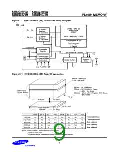
256M x 8 Bit / 128M x 16 Bit NAND Flash Memory
PRODUCT LIST
Part Number
K9K2G08Q0M-Y,P
K9K2G16Q0M-Y,P
K9XXG08UXM-Y,P,K,E
K9XXG16UXM-Y,P,K,E
K9K2G08U0M-V,F
Vcc Range
Organization
PKG Type
X8
X16
X8
1.7 ~ 1.95V
TSOP1
2.7 ~ 3.6V
X16
X8
WSOP1
FEATURES
• Voltage Supply
• Fast Write Cycle Time
-1.8V device(K9K2GXXQ0M): 1.7V~1.95V
-3.3V device(K9XXGXXUXM): 2.7 V ~3.6 V
- Program time : 300µs(Typ.)
- Block Erase Time : 2ms(Typ.)
• Organization
- Memory Cell Array
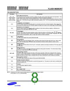
• Command/Address/Data Multiplexed I/O Port
• Hardware Data Protection
-X8 device(K9K2G08X0M) : (256M + 8,192K)bit x 8bit
-X16 device(K9K2G16X0M) : (128M + 4,096K)bit x 16bit
- Data Register
-X8 device(K9K2G08X0M): (2K + 64)bit x8bit
-X16 device(K9K2G16X0M): (1K + 32)bit x16bit
- Cache Register
-X8 device(K9K2G08X0M): (2K + 64)bit x8bit
-X16 device(K9K2G16X0M): (1K + 32)bit x16bit
• Automatic Program and Erase
- Page Program
- Program/Erase Lockout During Power Transitions
• Reliable CMOS Floating-Gate Technology
- Endurance : 100K Program/Erase Cycles
- Data Retention : 10 Years
• Command Register Operation
• Cache Program Operation for High Performance Program
• Power-On Auto-Read Operation
• Intelligent Copy-Back Operation
• Unique ID for Copyright Protection
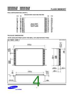
• Package :
-X8 device(K9K2G08X0M): (2K + 64)Byte
-X16 device(K9K2G16X0M): (1K + 32)Word
- Block Erase
- K9K2GXXX0M-YCB0/YIB0
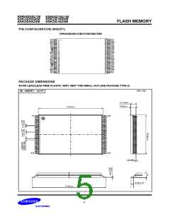
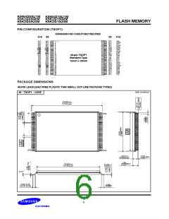
48 - Pin TSOP I (12 x 20 / 0.5 mm pitch)
- K9K2G08U0M-VCB0/VIB0
-X8 device(K9K2G08X0M): (128K + 4K)Byte
-X16 device(K9K2G16X0M): (64K + 2K)Word
• Page Read Operation
48 - Pin WSOP I (12X17X0.7mm)
- K9K2GXXX0M-PCB0/PIB0
48 - Pin TSOP I (12 x 20 / 0.5 mm pitch)- Pb-free Package
- K9K2G08U0M-FCB0/FIB0
- Page Size
- X8 device(K9K2G08X0M): 2K-Byte
- X16 device(K9K2G16X0M) : 1K-Word
- Random Read : 25µs(Max.)
- Serial Access
1.8V device(K9K2GXXQ0M): 80ns(Min.)
3.3V device(K9XXGXXUXM): 50ns(Min.)
48 - Pin WSOP I (12X17X0.7mm)- Pb-free Package
* K9K2G08U0M-V,F(WSOPI ) is the same device as
K9K2G08U0M-Y,P(TSOP1) except package type.
- K9W4GXXU1M-YCB0,PCB0/YIB0,PIB0 : Two K9K2G08U0M
stacked.
48 - Pin TSOP I (12 x 20 / 0.5 mm pitch)
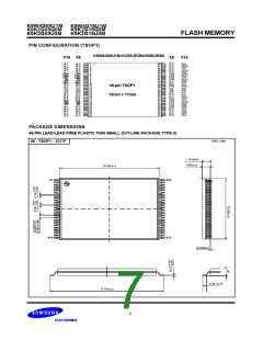
- K9W4GXXU1M-KCB0,ECB0/KIB0,EIB0 : Two K9K2G08U0M
stacked.
48 - Pin TSOP I (12 x 17 / 0.5 mm pitch)
GENERAL DESCRIPTION
Offered in 256Mx8bit or 128Mx16bit, the K9K2GXXX0M is 2G bit with spare 64M bit capacity. Its NAND cell provides the most cost-
effective solution for the solid state mass storage market. A program operation can be performed in typical 300µs on the 2112-byte(X8
device) or 1056-word(X16 device) page and an erase operation can be performed in typical 2ms on a 128K-byte(X8 device) or 64K-
word(X16 device) block. Data in the data page can be read out at 80ns(1.8V device) or 50ns(3.3V device) cycle time per byte(X8
device) or word(X16 device). The I/O pins serve as the ports for address and data input/output as well as command input. The on-chip
write controller automates all program and erase functions including pulse repetition, where required, and internal verification and
margining of data. Even the write-intensive systems can take advantage of the K9K2GXXX0M′s extended reliability of 100K program/
erase cycles by providing ECC(Error Correcting Code) with real time mapping-out algorithm. The K9K2GXXX0M is an optimum solu-
tion for large nonvolatile storage applications such as solid state file storage and other portable applications requiring non-volatility.
An ultra high density solution having two 2Gb stacked with two chip selects is also available in standard TSOPI package.
3

 SAMSUNG [ SAMSUNG ]