K9F5608Q0C
K9F5608D0C
K9F5608U0C
K9F5616Q0C
K9F5616D0C
K9F5616U0C
FLASH MEMORY
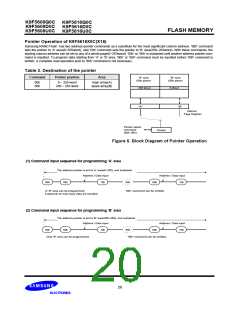
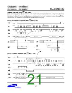
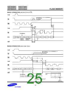
System Interface Using CE don’t-care.
For an easier system interface, CE may be inactive during the data-loading or sequential data-reading as shown below. The internal
528byte(x8 device), 264word(x16 device) page registers are utilized as seperate buffers for this operation and the system design gets
more flexible. In addition, for voice or audio applications which use slow cycle time on the order of u-seconds, de-activating CE during
the data-loading and reading would provide significant savings in power consumption.
Figure 6. Program Operation with CE don’t-care.
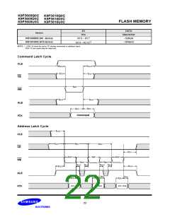
CLE
CE don’t-care
CE
WE
ALE
I/Ox
80h
Start Add.(3Cycle)
Data Input
Data Input
10h
tCS
tCH
tCEA
CE
RE
CE
tREA
tWP
tOH
WE
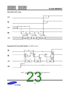
I/O0~15
out
Figure 7. Read Operation with CE don’t-care.
CLE
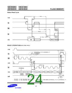
On K9F5608U0C_Y,P,V,F or K9F5608D0C_Y,P
CE must be held
CE don’t-care
low during tR
CE
RE
ALE
tR
R/B
WE
I/Ox
Data Output(sequential)
00h
Start Add.(3Cycle)
21

 SAMSUNG [ SAMSUNG ]