K9F5608Q0C
K9F5608D0C
K9F5608U0C
K9F5616Q0C
K9F5616D0C
K9F5616U0C
FLASH MEMORY
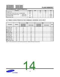
AC CHARACTERISTICS FOR OPERATION
Min
Max
K9F5608X0C
K9F5616U0C
K9F5616D0C
K9F5608X0C
K9F5616U0C
K9F5616D0C
Parameter
Symbol
Unit
K9F5616Q0C
K9F5616Q0C
Data Transfer from Cell to Register
ALE to RE Delay
tR
tAR
-
10
10
20
25
-
-
10
10
ms
ns
ns
ns
ns
ns
ns
ns
ns
ns
ns
ns
ns
ns
ns
ns
ms
10
10
20
40
-
-
-
CLE to RE Delay
tCLR
tRR
-
-
Ready to RE Low
-
-
RE Pulse Width
tRP
-
-
WE High to Busy
tWB
tRC
100
100
Read Cycle Time
50
-
60
-
-
-
30/35(1)
RE Access Time
tREA
tCEA
tRHZ
tCHZ
tOH
40
CE Access Time
-
-
45
55
RE High to Output Hi-Z
CE High to Output Hi-Z
RE or CE High to Output hold
RE High Hold Time
Output Hi-Z to RE Low
WE High to RE Low
-
-
30
30
-
-
20
20
15
15
0
15
20
0
-
-
tREH
tIR
-
-
-
-
tWHR1
60
100
-
60
-
-
WE High to RE Low in Block Lcok Mode tWHR2
Device Resetting Time(Read/Program/Erase)
100
-
-
5/10/500(2)
5/10/500(2)
-
tRST
Symbol
tRB
Min
Max
Uni
ns
K9F5608U0C-
Y,P,V,F or
K9F5608D0C-
Y,P only
Last RE High to Busy(at sequential read)
-
-
100
50 +tr(R/B)(3)
-
CE High to Ready(in case of interception by CE at
CE High Hold Time(at the last serial read)(4)
tCRY
ns
tCEH
100
ns
NOTE: 1. K9F5608Q0C tREA = 35ns.
2. If reset command(FFh) is written at Ready state, the device goes into Busy for maximum 5us.
3. The time to Ready depends on the value of the pull-up resistor tied R/B pin.
4. To break the sequential read cycle, CE must be held high for longer time than tCEH.
15

 SAMSUNG [ SAMSUNG ]