K9F1208Q0A K9F1216Q0A
K9F1208D0A K9F1216D0A
K9F1208U0A K9F1216U0A
FLASH MEMORY
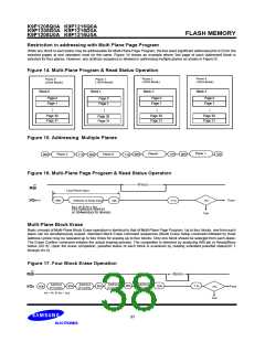
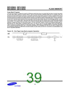
Restriction in addressing with Multi Plane Page Program
While any block in each plane may be addressable for Multi-Plane Page Program, the five least significant addresses(A9-A13) for the
selected pages at one operation must be the same. Figure 14 shows an example where 2nd page of each addressed block is
selected for four planes. However, any arbitrary sequence is allowed in addressing multiple planes as shown in Figure15.
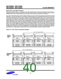
Figure 14. Multi-Plane Program & Read Status Operation
Plane 3
(1024 Block)
Plane 2
(1024 Block)
Plane 1
(1024 Block)
Plane 0
(1024 Block)
Block 0
Block 2
Block 3
Block 1
Page 0
Page 1
Page 0
Page 1
Page 0
Page 1
Page 0
Page 1
Page 30
Page 31
Page 30
Page 31
Page 30
Page 31
Page 30
Page 31
Figure 15. Addressing Multiple Planes
Plane 1
Plane3
80h
10h
Plane 2
Plane 0
80h
11h
80h
11h
80h
11h
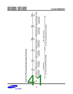
Figure 16. Multi-Plane Page Program & Read Status Operation
tPROG
R/B
Last Plane input
Pass
I/O0~7
80h
Address & Data Input
I/O
10h
71h
A0 ~ A7 & A9 ~ A25
528 bytes(x8 device)
or 264words(x16 device)
Fail
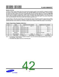
Multi-Plane Block Erase
Basic concept of Multi-Plane Block Erase operation is identical to that of Multi-Plane Page Program. Up to four blocks, one from each
plane can be simultaneously erased. Standard Block Erase command sequences (Block Erase Setup command followed by three
address cycles) may be repeated up to four times for erasing up to four blocks. Only one block should be selected from each plane.
The Erase Confirm command initiates the actual erasing process. The completion is detected by analyzing R/B pin or Ready/Busy
status (I/O 6). Upon the erase completion, pass/fail status of each block is examined by reading extended pass/fail status(I/O 1
through I/O 4).
Figure 17. Four Block Erase Operation
R/B
I/OX
tBERS
Address
(3 Cycle)
Address
(3 Cycle)
Address
(3 Cycle)
Address
(3 Cycle)
60h
60h
60h
D0h
71h
60h
Pass
I/O
A0 ~ A7 & A9 ~ A25
Fail
37

 SAMSUNG [ SAMSUNG ]