K9F1208Q0A K9F1216Q0A
K9F1208D0A K9F1216D0A
K9F1208U0A K9F1216U0A
FLASH MEMORY
BLOCK ERASE
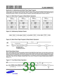
The Erase operation is done on a block(16K Byte) basis. Block address loading is accomplished in three cycles initiated by an Erase
Setup command(60h). Only address A14 to A25 is valid while A9 to A13 is ignored. The Erase Confirm command(D0h) following the
block address loading initiates the internal erasing process. This two-step sequence of setup followed by execution command
ensures that memory contents are not accidentally erased due to external noise conditions.
At the rising edge of WE after the erase confirm command input, the internal write controller handles erase and erase-verify. When
the erase operation is completed, the Write Status Bit(I/O 0) may be checked. Figure 12 details the sequence.
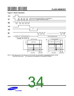
Figure 12. Block Erase Operation
tBERS
R/B
Pass
I/OX
60h
I/O0
Fail
70h
Address Input(3Cycle)
Block Add. : A14 ~ A25
D0h
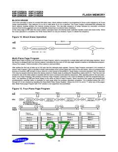
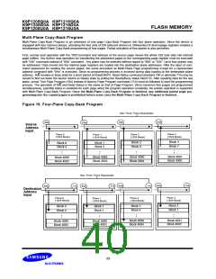
Multi-Plane Page Program
Multi-Plane Page Program is an extension of Page Program, which is executed for a single plane with 528 byte page registers. Since
the device is equipped with four memory planes, activating the four sets of 528 byte page registers enables a simultaneous program-
ming of four pages. Partial activation of four planes is also permitted.
After writing the first set of data up to 528 byte into the selected page register, Dummy Page Program command (11h) instead of
actual Page Program (10h) is inputted to finish data-loading of the current plane and move to the next plane. Since no programming
process is involved, R/B remains in Busy state for a short period of time(tDBSY). Read Status command (standard 70h or alternate
71h) may be issued to find out when the device returns to Ready state by polling the Ready/Busy status bit(I/O 6). Then the next set
of data for one of the other planes is inputted with the same command and address sequences. After inputting data for the last plane,
actual True Page Program (10h) instead of dummy Page Program command (11h) must be followed to start the programming pro-
cess. The operation of R/B and Read Status is the same as that of Page Program. Since maximum four pages are programmed
simultaneously, pass/fail status is available for each page when the program operation completes. The extended status bits (I/O1
through I/O 4) are checked by inputting the Read Multi-Plane Status Register. Status bit of I/O 0 is set to "1" when any of the pages
fails. Multi-Plane page Program with "01h" pointer is not supported, thus prohibited.
Figure 13. Four-Plane Page Program
tDBSY
tPROG
10h
tDBSY
11h
tDBSY
11h
R/B
I/OX
Address &
Data Input
Address &
Data Input
Address &
Data Input
A0 ~ A7 & A9 ~ A25
Address &
Data Input
71h
80h
80h
80h
80h
80h
80h
11h
80h
80h
528 bytes(x8 device)
or 264words(x16 device)
10h
11h
11h
11h
Data
Input
Plane 3
(1024 Block)
Plane 0
(1024 Block)
Plane 2
(1024 Block)
Plane 1
(1024 Block)
Block 3
Block 7
Block 2
Block 6
Block 1
Block 5
Block 0
Block 4
Block 4091
Block 4095
Block 4090
Block 4094
Block 4089
Block 4093
Block 4088
Block 4092
36

 SAMSUNG [ SAMSUNG ]