DDR SDRAM 256Mb E-die (x4, x8)
DDR SDRAM
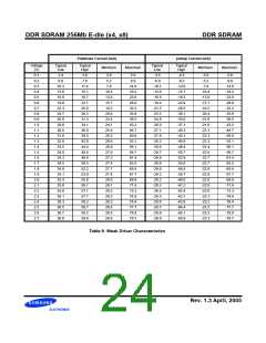
System Notes :
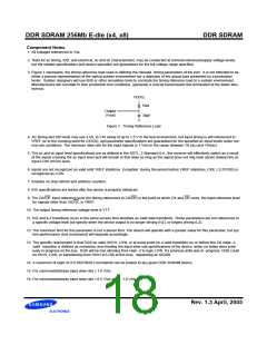
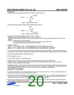
a. Pullup slew rate is characteristized under the test conditions as shown in Figure 2.
Test point
Output
50Ω
VSSQ
Figure 2 : Pullup slew rate test load
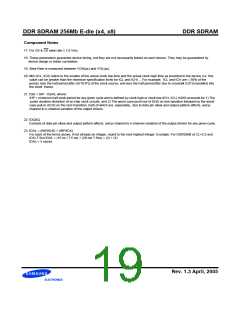
b. Pulldown slew rate is measured under the test conditions shown in Figure 3.
VDDQ
50Ω
Output
Test point
Figure 3 : Pulldown slew rate test load
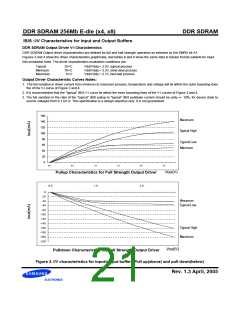
c. Pullup slew rate is measured between (VDDQ/2 - 320 mV +/- 250 mV)
Pulldown slew rate is measured between (VDDQ/2 + 320 mV +/- 250 mV)
Pullup and Pulldown slew rate conditions are to be met for any pattern of data, including all outputs switching and only one output
switching.
Example : For typical slew rate, DQ0 is switching
For minmum slew rate, all DQ bits are switching from either high to low, or low to high.
The remaining DQ bits remain the same as for previous state.
d. Evaluation conditions
Typical : 25 °C (T Ambient), VDDQ = 2.5V(for DDR266/333) and 2.6V(for DDR400), typical process
Minimum : 70 °C (T Ambient), VDDQ = 2.3V(for DDR266/333) and 2.5V(for DDR400), slow - slow process
Maximum : 0 °C (T Ambient), VDDQ = 2.7V(for DDR266/333) and 2.7V(for DDR400), fast - fast process
e. The ratio of pullup slew rate to pulldown slew rate is specified for the same temperature and voltage, over the entire temperature and
voltage range. For a given output, it represents the maximum difference between pullup and pulldown drivers due to process variation.
f. Verified under typical conditions for qualification purposes.
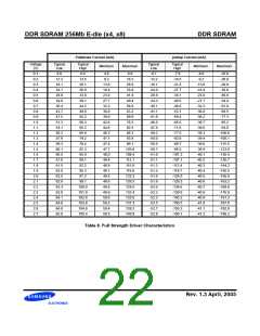
g. TSOPII package divices only.
h. Only intended for operation up to 266 Mbps per pin.
i. A derating factor will be used to increase tIS and tIH in the case where the input slew rate is below 0.5V/ns
as shown in Table 2. The Input slew rate is based on the lesser of the slew rates detemined by either VIH(AC) to VIL(AC) or
VIH(DC) to VIL(DC), similarly for rising transitions.
j. A derating factor will be used to increase tDS and tDH in the case where DQ, DM, and DQS slew rates differ, as shown in Tables 3 & 4.
Input slew rate is based on the larger of AC-AC delta rise, fall rate and DC-DC delta rise, Input slew rate is based on the lesser of the
slew rates determined by either VIH(AC) to VIL(AC) or VIH(DC) to VIL(DC), similarly for rising transitions.
The delta rise/fall rate is calculated as:
{1/(Slew Rate1)} - {1/(Slew Rate2)}
For example : If Slew Rate 1 is 0.5 V/ns and slew Rate 2 is 0.4 V/ns, then the delta rise, fall rate is - 0.5ns/V . Using the table given, this
would result in the need for an increase in tDS and tDH of 100 ps.
k. Table 3 is used to increase tDS and tDH in the case where the I/O slew rate is below 0.5 V/ns. The I/O slew rate is based on the lesser
on the lesser of the AC - AC slew rate and the DC- DC slew rate. The inut slew rate is based on the lesser of the slew rates deter
mined by either VIH(ac) to VIL(ac) or VIH(DC) to VIL(DC), and similarly for rising transitions.
m. DQS, DM, and DQ input slew rate is specified to prevent double clocking of data and preserve setup and hold times. Signal transi
tions through the DC region must be monotonic.
Rev. 1.3 April, 2005

 SAMSUNG [ SAMSUNG ]