DDR SDRAM 256Mb E-die (x4, x8)
DDR SDRAM
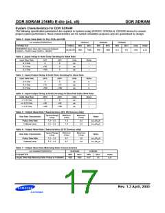
Component Notes
1. All voltages referenced to Vss.
2. Tests for ac timing, IDD, and electrical, ac and dc characteristics, may be conducted at nominal reference/supply voltage levels,
but the related specifications and device operation are guaranteed for the full voltage range specified.
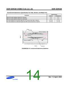
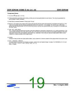
3. Figure 1 represents the timing reference load used in defining the relevant timing parameters of the part. It is not intended to be
either a precise representation of the typical system environment nor a depiction of the actual load presented by a production
tester. System designers will use IBIS or other simulation tools to correlate the timing reference load to a system environment.
Manufacturers will correlate to their production test conditions (generally a coaxial transmission line terminated at the tester elec-
tronics).
VDDQ
50Ω
Output
(Vout)
30pF
Figure 1 : Timing Reference Load
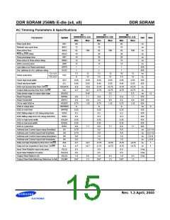
4. AC timing and IDD tests may use a VIL to VIH swing of up to 1.5 V in the test environment, but input timing is still referenced to
VREF (or to the crossing point for CK/CK), and parameter specifications are guaranteed for the specified ac input levels under nor-
mal use conditions. The minimum slew rate for the input signals is 1 V/ns in the range between VIL(ac) and VIH(ac).
5. The ac and dc input level specifications are as defined in the SSTL_2 Standard (i.e., the receiver will effectively switch as a result
of the signal crossing the ac input level and will remain in that state as long as the signal does not ring back above (below) the dc
input LOW (HIGH) level.
6. Inputs are not recognized as valid until VREF stabilizes. Exception: during the period before VREF stabilizes, CKE ≤ 0.2VDDQ is
recognized as LOW.
7. Enables on.chip refresh and address counters.
8. IDD specifications are tested after the device is properly initialized.
9. The CK/CK input reference level (for timing referenced to CK/CK) is the point at which CK and CK cross; the input reference level
for signals other than CK/CK, is VREF.
10. The output timing reference voltage level is VTT.
11. tHZ and tLZ transitions occur in the same access time windows as valid data transitions. These parameters are not referenced to
a specific voltage level but specify when the device output is no longer driving (HZ), or begins driving (LZ).
12. The maximum limit for this parameter is not a device limit. The device will operate with a greater value for this parameter, but sys
tem performance (bus turnaround) will degrade accordingly.
13. The specific requirement is that DQS be valid (HIGH, LOW, or at some point on a valid transition) on or before this CK edge. A
valid transition is defined as monotonic and meeting the input slew rate specifications of the device. when no writes were previ
ously in progress on the bus, DQS will be tran sitioning from High- Z to logic LOW. If a previous write was in progress, DQS could
be HIGH, LOW, or transitioning from HIGH to LOW at this time, depending on tDQSS.
14. A maximum of eight AUTO REFRESH commands can be posted to any given DDR SDRAM device.
15. For command/address input slew rate ≥ 1.0 V/ns
16. For command/address input slew rate ≥ 0.5 V/ns and < 1.0 V/ns
Rev. 1.3 April, 2005

 SAMSUNG [ SAMSUNG ]