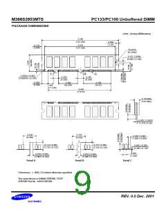
M366S2953MTS
PC133/PC100 Unbuffered DIMM
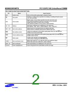
PIN CONFIGURATION DESCRIPTION
Pin
Name
System clock
Input Function
CLK
CS
Active on the positive going edge to sample all inputs.
Disables or enables device operation by masking or enabling all inputs except
CLK, CKE and DQM.
Chip select
Masks system clock to freeze operation from the next clock cycle.
CKE should be enabled at least one cycle prior to new command.
Disable input buffers for power down in standby.
CKE
Clock enable
CKE should be enabled 1CLK+tSS prior to valid command.
Row/column addresses are multiplexed on the same pins.
Row address : RA0 ~ RA12, Column address : CA0 ~ CA9,CA11
A0 ~ A12
BA0 ~ BA1
RAS
Address
Selects bank to be activated during row address latch time.
Selects bank for read/write during column address latch time.
Bank select address
Row address strobe
Column address strobe
Write enable
Latches row addresses on the positive going edge of the CLK with RAS low.
Enables row access & precharge.
Latches column addresses on the positive going edge of the CLK with CAS low.
Enables column access.
CAS
Enables write operation and row precharge.
Latches data in starting from CAS, WE active.
WE
Makes data output Hi-Z, tSHZ after the clock and masks the output.
Blocks data input when DQM active. (Byte masking)
DQM0 ~ 7
Data input/output mask
DQ0 ~ 63
VDD/VSS
Data input/output
Data inputs/outputs are multiplexed on the same pins.
Power and ground for the input buffers and the core logic.
Power supply/ground
REV. 0.0 Dec. 2001

 SAMSUNG [ SAMSUNG ]