Datasheet
RGSX5TS65E
lIGBT Electrical Characteristics (at Tj = 25°C unless otherwise specified)
Values
Typ.
2320
168
23
Parameter
Symbol
Conditions
Unit
pF
Min.
Max.
Cies VCE = 30V
Coes VGE = 0V
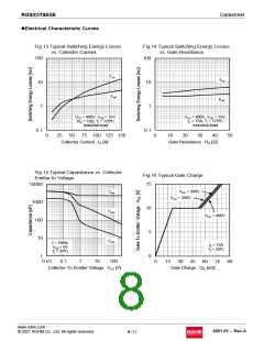
Input Capacitance
Output Capacitance
Reverse transfer Capacitance
Total Gate Charge
Gate - Emitter Charge
Gate - Collector Charge
Turn - on Delay Time
Rise Time
-
-
-
-
-
-
-
-
-
-
-
-
-
-
-
-
-
-
-
-
-
-
-
-
-
-
-
-
-
-
-
-
-
-
-
-
Cres
Qg
f = 1MHz
VCE = 300V
79
Qge IC = 75A
Qgc VGE = 15V
td(on)
21
nC
33
43
IC = 75A, VCC = 400V,
VGE = 15V, RG = 10Ω,
Tj = 25°C
Inductive Load
*Eon include diode
reverse recovery
tr
td(off)
tf
40
ns
mJ
ns
Turn - off Delay Time
Fall Time
113
87
Eon
Eoff
td(on)
tr
Turn-on Switching Loss
Turn-off Switching Loss
Turn - on Delay Time
Rise Time
3.44
1.90
42
IC = 75A, VCC = 400V,
VGE = 15V, RG = 10Ω,
Tj = 175°C
Inductive Load
*Eon include diode
reverse recovery
45
td(off)
tf
Turn - off Delay Time
Fall Time
135
137
3.72
2.58
Eon
Eoff
Turn-on Switching Loss
Turn-off Switching Loss
mJ
-
IC = 225A, VCC = 520V
Vp = 650V, VGE = 15V
RG = 50Ω, Tj = 175°C
Reverse Bias
Safe Operating Area
RBSOA
tsc
FULL SQUARE
V
CC ≤ 360V
VGE = 15V, Tj = 25°C
Short Circuit Withstand Time
Short Circuit Withstand Time
8
6
-
-
-
-
μs
μs
V
CC ≤ 360V
VGE = 15V, Tj = 150°C
*2
tsc
*2 Design assurance without measurement
www.rohm.com
© 2021 ROHM Co., Ltd. All rights reserved.
2021.01 - Rev.A
3/11

 ROHM [ ROHM ]