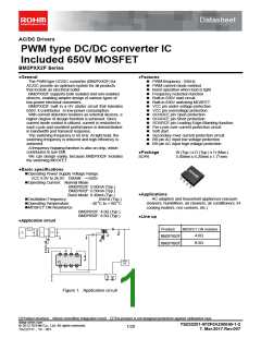
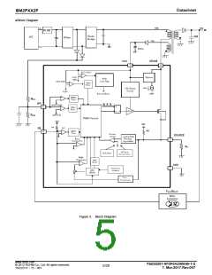
Daattaasshheeeett
BM2PXX2F
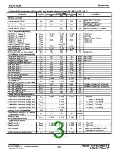
●Electrical Characteristics of Control IC part (Unless otherwise noted, Ta = 25C, VCC = 15 V)
Specifications
Parameter
Symbol
Unit
Conditions
Min
Typ
Max
[BR pin function]
BR UVLO detection voltage1
BR UVLO voltage 2
BR UVLO hysteresis
BR UVLO detection delay time1
BR UVLO detection delay time2
BR OVP detection voltage1
BR OVP detection valtage2
BR OVP hysteresis
VBR1
VBR2
VBR3
TBR1
TBR2
VBR4
VBR5
VBR6
TBR3
TBR4
0.45
0.29
-
0.50
0.35
0.15
100
0.55
0.41
-
150
350
2.20
2.10
-
V
V
V
us
ms
V
V
V
us
us
BR rises
BR falls
VBR3=VBR1-VBR2
BR rises
BR falls
BR rises
BR falls
VBR6=VBR4-VBR5
BR rises
BR falls
50
150
2.00
1.90
-
50
50
256
2.10
2.00
0.10
100
BR OVP detection delay time1
BR OVP detection delay time2
150
150
100
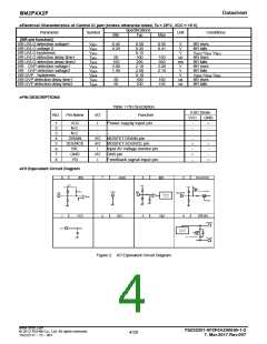
●PIN DESCRIPTIONS
Table 1 Pin Description
Function
ESD Diode
NO.
Pin Name
I/O
VCC
GND
1
2
3
4
5
6
7
8
VCC
N.C.
I
-
Power supply input pin
-
-
-
○
-
N.C.
-
-
-
-
DRAIN
SOURCE
BR.
I/O
I/O
I
MOSFET DRAIN pin
MOSFET SOURCE pin
Input AV Voltage monitor pin
GND pin
-
-
○
-
○
-
GND
I/O
I
○
-
-
FB
Feedback signal input pin
○
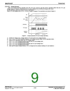
●I/O Equivalent Circuit Diagram
Figure 2. I/O Equivalent Circuit Diagram
www.rohm.com
© 2012 ROHM Co., Ltd. All rights reserved.
TSZ22111・15・001
TSZ02201-0F2F0A200040-1-2
7. Mar.2017.Rev.007
4/20

 ROHM [ ROHM ]