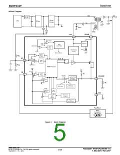
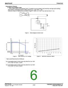
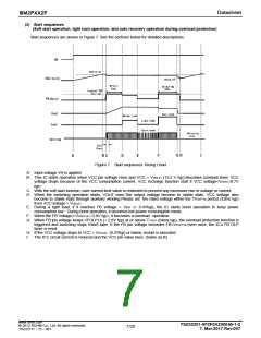
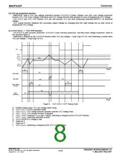
Daattaasshheeeett
BM2PXX2F
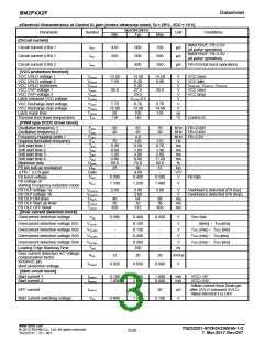
●Electrical Characteristics of Control IC part (Unless otherwise noted, Ta = 25C, VCC = 15 V)
Specifications
Parameter
[Circuit current]
Symbol
Unit
Conditions
Min
Typ
Max
BM2P052F, FB=2.0V
(at pulse operation)
BM2P092F, FB=2.0V
(at pulse operation)
Circuit current (ON) 1
Circuit current (ON) 1
ION1
ION1
ION2
410
350
-
600
500
400
790
650
500
μA
μA
μA
Circuit current (ON) 2
FB=0.0V(at burst operation)
[VCC protection function]
VCC UVLO voltage 1
VCC UVLO voltage 2
VCC UVLO hysteresis
VCC OVP voltage 1
VCC OVP voltage 2
Latch released VCC voltage
VCC Recharge start voltage
VCC Recharge stop voltage
Latch mask time
VUVLO1
VUVLO2
VUVLO3
VOVP1
VOVP2
VLATCH
VCHG1
VCHG2
TLATCH
TSD
12.50
7.50
-
13.50
8.20
5.30
27.5
23.5
VUVLO2-0.5
8.70
13.00
100
145
14.50
8.90
-
V
V
V
V
V
V
V
V
us
C
VCC rises
VCC falls
VUVLO3= VUVLO1- VUVLO2
VCC rises
VCC drop
26.0
29.0
-
-
7.70
12.00
50
9.70
14.00
150
-
Thermal shut down temperature
118
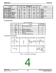
Control IC
[PWM type DCDC driver block]
Oscillation frequency 1
Oscillation frequency 2
Frequency hopping width 1
Hopping fluctuation frequency
Soft start time 1
Soft start time 2
Soft start time 3
Soft start time 4
Maximum duty
FSW1
FSW2
FDEL1
FCH
TSS1
TSS2
TSS3
TSS4
Dmax
RFB
60
20
-
65
25
4.0
125
0.50
1.00
2.00
8.00
75.0
30
70
30
-
175
0.70
1.40
2.80
11.20
82.0
37
KHz FB=2.00V
KHz FB=0.40V
KHz FB=2.0V
Hz
ms
ms
ms
ms
%
75
0.30
0.60
1.20
4.80
68.0
23
FB pin pull-up resistance
ΔFB / ΔCS gain
FB burst voltage
kΩ
V/V
Gain
VBST
-
4.00
0.400
-
0.300
0.500
V
FB falls
FB voltage of
VDLT
1.100
1.250
1.400
V
starting Frequency reduction mode
FB OLP voltage 1a
FB OLP voltage 1b
FB OLP ON timer
FB OLP Start up timer
FB OLP OFF timer
VFOLP1A
VFOLP1B
TFOLP1
TFOLP1b
TFOLP2
2.60
-
40
26
358
2.80
2.60
64
32
512
3.00
-
88
38
666
V
V
ms
ms
ms
Overload is detected (FB rise)
Overload is detected (FB drop)
[Over current detection block]
Overcurrent detection voltage
VCS
0.380
0.400
0.100
0.150
0.200
0.300
250
0.420
V
V
Ton=0us
Overcurrent detection voltage SS1
Overcurrent detection voltage SS2
Overcurrent detection voltage SS3
Overcurrent detection voltage SS4
Leading Edge Blanking Time
VCS_SS1
VCS_SS2
VCS_SS3
VCS_SS4
TLEB
-
-
-
-
-
-
-
-
-
-
0[ms] ~ TSS1[ms]
TSS1 [ms] ~ TSS2 [ms]
TSS2 [ms] ~ TSS3[ms]
TSS3 [ms] ~ TSS4 [ms]
V
V
V
ns
Over current detection AC Voltage
compensation factor
SOURCE pin
KCS
12
20
28
mV/us
V
VCSSHT
0.020
0.050
0.080
short protection voltage
[Start circuit block]
Start current 1
Start current 2
ISTART1
ISTART2
0.100
1.000
0.500
3.000
1.000
6.000
mA
mA
VCC= 0V
VCC=10V
Inflow current from Drain pin
after UVLO released UVLO.
When MOSFET is OFF
OFF current
ISTART3
VSC
-
10
20
uA
V
Start current switching voltage
0.800
1.500
2.100
www.rohm.com
TSZ02201-0F2F0A200040-1-2
7. Mar.2017.Rev.007
© 2012 ROHM Co., Ltd. All rights reserved.
3/20
TSZ22111・15・001

 ROHM [ ROHM ]