BD9A300MUV
Operational Notes
1.
2.
Reverse Connection of Power Supply
Connecting the power supply in reverse polarity can damage the IC. Take precautions against reverse polarity when
connecting the power supply, such as mounting an external diode between the power supply and the IC’s power
supply pins.
Power Supply Lines
Design the PCB layout pattern to provide low impedance supply lines. Separate the ground and supply lines of the
digital and analog blocks to prevent noise in the ground and supply lines of the digital block from affecting the analog
block. Furthermore, connect a capacitor to ground at all power supply pins. Consider the effect of temperature and
aging on the capacitance value when using electrolytic capacitors.
3.
4.
Ground Voltage
Ensure that no pins are at a voltage below that of the ground pin at any time, even during transient condition.
OR
Ground Wiring Pattern
When using both small-signal and large-current ground traces, the two ground traces should be routed separately but
connected to a single ground at the reference point of the application board to avoid fluctuations in the small-signal
ground caused by large currents. Also ensure that the ground traces of external components do not cause variations
on the ground voltage. The ground lines must be as short and thick as possible to reduce line impedance.
5.
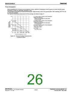
Thermal Consideration
Should by any chance the power dissipation rating be exceeded the rise in temperature of the chip may result in
deterioration of the properties of the chip. The absolute maximum rating of the Pd stated in this specification is when
the IC is mounted on a 70mm x 70mm x 1.6mm 4-layer glass epoxy board. In case of exceeding this absolute
maximum rating increase the board size and copper area to prevent exceeding the Pd rating.
6.
7.
Recommended Operating Conditions
These conditions represent a range within which the expected characteristics of the IC can be approximately obtained.
The electrical characteristics are guaranteed under the conditions of each parameter.
Inrush Current
When power is first supplied to the IC, it is possible that the internal logic may be unstable and inrush current may
flow instantaneously due to the internal powering sequence and delays, especially if the IC has more than one power
supply. Therefore, give special consideration to power coupling capacitance, power wiring, width of ground wiring, and
routing of connections.
8.
9.
Operation Under Strong Electromagnetic Field
Operating the IC in the presence of a strong electromagnetic field may cause the IC to malfunction.
Testing on Application Boards
When testing the IC on an application board, connecting a capacitor directly to a low-impedance output pin may
subject the IC to stress. Always discharge capacitors completely after each process or step. The IC’s power supply
should always be turned off completely before connecting or removing it from the test setup during the inspection
process. To prevent damage from static discharge, ground the IC during assembly and use similar precautions during
transport and storage.
10. Inter-pin Short and Mounting Errors
Ensure that the direction and position are correct when mounting the IC on the PCB. Incorrect mounting may result in
damaging the IC. Avoid nearby pins being shorted to each other especially to ground, power supply and output pin.
Inter-pin shorts could be due to many reasons such as metal particles, water droplets (in very humid environment) and
unintentional solder bridge deposited in between pins during assembly to name a few.
www.rohm.com
TSZ02201-0J3J0AJ00350-1-2
30.Jun.2017 Rev.003
© 2013 ROHM Co., Ltd. All rights reserved.
28/32
TSZ22111・15・001

 ROHM [ ROHM ]