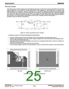
BD9A300MUV
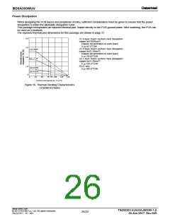
Power Dissipation
When designing the PCB layout and peripheral circuitry, sufficient consideration must be given to ensure that the power
dissipation is within the allowable dissipation curve.
This package incorporates an exposed thermal pad. Solder directly to the PCB ground plane. After soldering, the PCB can
be used as a heatsink.
The exposed thermal pad dimensions for this package are shown in page 31.
4.0
(1) 4-layer board (surface heat dissipation
copper foil 5505mm2)
(copper foil laminated on each layer)
JA=47.0°C/W
3.0
2.0
(2) 4-layer board (surface heat dissipation
[1] 2.66W
[2] 1.77W
copper foil 6.28mm2)
(copper foil laminated on each layer)
JA=70.62°C/W
(3) 1-layer board (surface heat dissipation
copper foil 6.28mm2)
JA=201.6°C/W
(4) IC only
1.0
0
[3] 0.62W
[4] 0.27W
JA=462.9°C/W
0
25
50
75 85 100
125
150
Ambient temperature: Ta [°C]
Figure 56. Thermal Derating Characteristics
(VQFN016V3030)
www.rohm.com
TSZ02201-0J3J0AJ00350-1-2
30.Jun.2017 Rev.003
© 2013 ROHM Co., Ltd. All rights reserved.
26/32
TSZ22111・15・001

 ROHM [ ROHM ]