BD9A300MUV
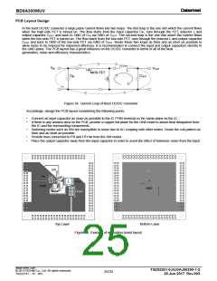
PCB Layout Design
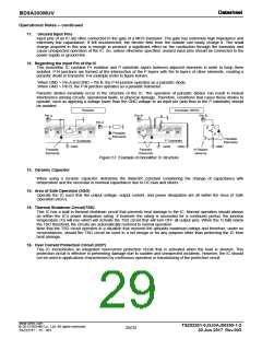
In the buck DC/DC converter a large pulse current flows into two loops. The first loop is the one into which the current flows
when the high-side FET is turned on. The flow starts from the input capacitor CIN, runs through the FET, inductor L and
output capacitor COUT and back to GND of CIN via GND of COUT. The second loop is the one into which the current flows
when the low-side FET is turned on. The flow starts from the low-side FET, runs through the inductor L and output capacitor
COUT and back to GND of the low-side FET via GND of COUT. Route these two loops as thick and as short as possible to
allow noise to be reduced for improved efficiency. It is recommended to connect the input and output capacitors directly to
the GND plane. The PCB layout has a great influence on the DC/DC converter in terms of all of the heat
generation, noise and efficiency characteristics.
VIN
VOUT
L
MOS FET
CIN
COUT
Figure 54. Current Loop of Buck DC/DC Converter
Accordingly, design the PCB layout considering the following points.
Connect an input capacitor as close as possible to the IC PVIN terminal on the same plane as the IC.
If there is any unused area on the PCB, provide a copper foil plane for the GND node to assist heat dissipation from
the IC and the surrounding components.
Switching nodes such as SW are susceptible to noise due to AC coupling with other nodes. Route the coil pattern as
thick and as short as possible.
Provide lines connected to FB and ITH far from the SW nodes.
Place the output capacitor away from the input capacitor in order to avoid the effect of harmonic noise from the input.
EN
CIN
VIN
L
VOUT
GND
GND
COUT
Top Layer
Bottom Layer
Figure 55. Example of evaluation board layout
www.rohm.com
TSZ02201-0J3J0AJ00350-1-2
30.Jun.2017 Rev.003
© 2013 ROHM Co., Ltd. All rights reserved.
25/32
TSZ22111・15・001

 ROHM [ ROHM ]