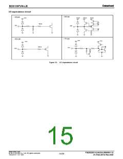
BD9109FVM-LB
Switching Regulator Efficiency
Efficiency ŋ may be expressed by the equation shown below:
VOUT×IOUT
Vin×Iin
POUT
POUT
η=
×100[%]=
×100[%]=
×100[%]
Pin
POUT+PDα
Efficiency may be improved by reducing the switching regulator power dissipation factors PDα as follows:
Dissipation factors:
1) ON resistance dissipation of inductor and FET:PD(I2R)
2) Gate charge/discharge dissipation:PD(Gate)
3) Switching dissipation:PD(SW)
4) ESR dissipation of capacitor:PD(ESR)
5) Operating current dissipation of IC:PD(IC)
2
1)PD(I2R)=IOUT ×(RCOIL+RON) (RCOIL[Ω]:DC resistance of inductor, RON[Ω]:ON resistance of FETIOUT[A]:Output current.)
2)PD(Gate)=Cgs×f×V2 (Cgs[F]:Gate capacitance of FET,f[Hz]:Switching frequency,V[V]:Gate driving voltage of FET)
Vin2×CRSS×IOUT×f
3)PD(SW)=
(CRSS[F]:Reverse transfer capacitance of FET、IDRIVE[A]:Peak current of gate.)
IDRIVE
2
4)PD(ESR)=IRMS ×ESR (IRMS[A]:Ripple current of capacitor,ESR[Ω]:Equivalent series resistance.)
5)PD(IC)=Vin×ICC (ICC[A]:Circuit current.)
Power Dissipation
As this IC functions with high efficiency without significant heat generation in most applications, no special consideration is
needed on permissible dissipation or heat generation. In case of extreme conditions, however, including lower input
voltage, higher output voltage, heavier load, and/or higher temperature, the permissible dissipation and/or heat generation
must be carefully considered.
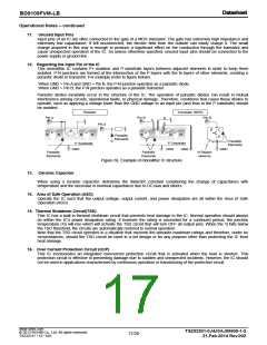
For dissipation, only conduction losses due to DC resistance of inductor and ON resistance of FET are considered.
Because the conduction losses are considered to play the leading role among other dissipation mentioned above including
gate charge/discharge dissipation and switching dissipation.
1000
2
①mounted on glass epoxy PCB
θja=212.8°C/W
P=IOUT ×(RCOIL+RON)
RON=D×RONP+(1-D)×RONN
②Using an IC alone
θja=322.6°C/W
800
D:ON duty (=VOUT/VCC)
RCOIL:DC resistance of coil
①587.4mW
②387.5mW
600
RONP:ON resistance of P-channel MOS FET
RONN:ON resistance of N-channel MOS FET
IOUT:Output current
400
200
0
0
25
50
75 85 100
125
150
Ambient temperature:Ta [℃]
Figure 34. Thermal derating curve
(MSOP8)
If VCC=5V, VOUT=3.3V, RCOIL=0.15Ω, RONP=0.35Ω, RONN=0.25Ω,IOUT=0.8A, for example,
D=VOUT/VCC=3.3/5=0.66
RON=0.66×0.35+(1-0.66)×0.25
=0.231+0.085
=0.316[Ω]
P=0.82×(0.15+0.316)
≒298[mV]
As RONP is greater than RONN in this IC, the dissipation increases as the ON duty becomes greater. With the
consideration on the dissipation as above, thermal design must be carried out with sufficient margin allowed.
www.rohm.com
TSZ02201-0J4J0AJ00600-1-2
21.Feb.2014 Rev.002
© 2013 ROHM Co., Ltd. All rights reserved.
14/20
TSZ22111 • 15 • 001

 ROHM [ ROHM ]