BD9109FVM-LB
Application Example
VOUT
ITH
VCC
PVCC
SW
1
2
3
4
8
7
6
5
VCC
RITH
CIN
①
L
EN
EN
VOUT
CITH
CO
GND
PGND
GND
②
③
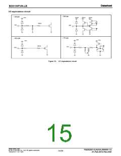
Figure 26. Board layout
For the sections drawn with heavy line, use thick conductor pattern as short as possible.
①
②
Lay out the input ceramic capacitor CIN closer to the pins PVCC and PGND, and the output capacitor Co closer to the
pin PGND.
③
Lay out CITH and RITH between the pins ITH and GND as neat as possible with least necessary wiring.
Recommended Component Lists With Above Applications
Symbol
Part
Value
Manufacturer
Sumida
TDK
Kyocera
Kyocera
murata
Series
CMD6D11B
VLF5014AT-4R7M1R1
CM316X5R106K10A
CM316X5R106K10A
GRM18 Series
L
Coil
4.7μH
Ceramic capacitor
Ceramic capacitor
Ceramic capacitor
Resistance
CIN
CO
10μF
10μF
330pF
30kΩ
CITH
RITH
Rohm
MCR10 3002
The parts list presented above is an example of recommended parts. Although the parts are sound, actual circuit characteristics should be checked on your
application carefully before use. Be sure to allow sufficient margins to accommodate variations between external devices and this IC when employing the
depicted circuit with other circuit constants modified. Both static and transient characteristics should be considered in establishing these margins. When
switching noise is substantial and may impact the system, a low pass filter should be inserted between the VCC and PVCC pins, and a schottky barrier
diode established between the SW and PGND pins.
www.rohm.com
TSZ02201-0J4J0AJ00600-1-2
21.Feb.2014 Rev.002
© 2013 ROHM Co., Ltd. All rights reserved.
11/20
TSZ22111 • 15 • 001

 ROHM [ ROHM ]