BD9109FVM-LB
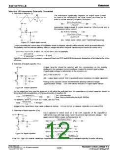
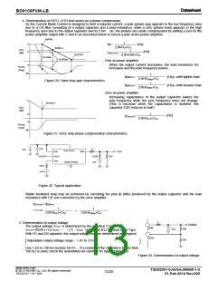
4. Determination of RITH, CITH that works as a phase compensator
As the Current Mode Control is designed to limit a inductor current, a pole (phase lag) appears in the low frequency area
due to a CR filter consisting of a output capacitor and a load resistance, while a zero (phase lead) appears in the high
frequency area due to the output capacitor and its ESR. So, the phases are easily compensated by adding a zero to the
power amplifier output with C and R as described below to cancel a pole at the power amplifier.
fp(Min)
1
2π×RO×CO
1
A
0
fp=
[Hz]
fp(Max)
Gain
[dB]
[Hz]
fz(ESR)=
fz(ESR)
2π×ESR×CO
IOUTMin
IOUTMax
Pole at power amplifier
0
When the output current decreases, the load resistance Ro
increases and the pole frequency lowers.
Phase
[deg]
-90
1
fp(Min)=
[Hz]←with lighter load
[Hz]←with heavier load
2π×ROMax×CO
Figure 30. Open loop gain characteristics
1
fp(Max)=
2π×ROMin×CO
Zero at power amplifier
Increasing capacitance of the output capacitor lowers the
pole frequency while the zero frequency does not change.
(This is because when the capacitance is doubled, the
capacitor ESR reduces to half.)
A
fz(Amp)
Gain
[dB]
0
0
1
[Hz]
2π×RITH×CITH
fz(Amp)=
Phase
[deg]
-90
Figure 31. Error amp phase compensation characteristics
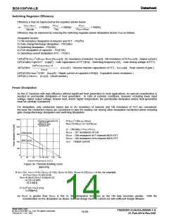
Cin
L
VCC
VCC,PVCC
EN
SW
VOUT
VOUT
VOUT
ITH
ESR
CO
RO
GND,PGND
RITH
CITH
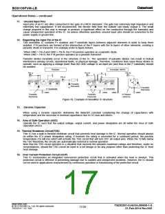
Figure 32. Typical application
Stable feedback loop may be achieved by canceling the pole fp (Min) produced by the output capacitor and the load
resistance with CR zero correction by the error amplifier.
fz(Amp)= fp(Min)
1
1
=
2π×RITH×CITH
2π×ROMax×CO
L
5. Determination of output voltage
Output
The output voltage VOUT is determined by the equation (7):
VOUT=(R2/R1+1)×VADJ・・・(7) VADJ: Voltage at ADJ terminal (0.8V Typ)
With R1 and R2 adjusted, the output voltage may be determined as required.
SW
Co
R2
R1
ADJ
Adjustable output voltage range:1.0V to 2.5V
Use 1 kΩ to 100 kΩ resistor for R1. If a resistor of the resistance higher than
100 kΩ is used, check the assembled set carefully for ripple voltage etc.
Figure 33. Determination of output voltage
www.rohm.com
TSZ02201-0J4J0AJ00600-1-2
21.Feb.2014 Rev.002
© 2013 ROHM Co., Ltd. All rights reserved.
13/20
TSZ22111 • 15 • 001

 ROHM [ ROHM ]