AD7228A
DACs for correct timing relationships during the calibration
cycle of the instrument.
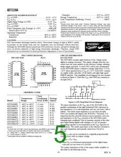
Figure 12. Self-Program m able Reference
Figure 10b. AD7228A Tim ing Deskew Circuit
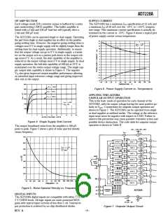
CO ARSE/FINE AD JUST
T he DACs on the AD7228A can be paired together to form a
coarse/fine adjust function as indicated in Figure 11. T he func-
tion is achieved using one external op amp and a few resistors
per pair of DACs.
DAC1 is the most significant or coarse DAC. Data is first
loaded to this DAC to coarsely set the output voltage. DAC2 is
then used to fine tune this output voltage. Varying the ratio of
R1 to R2 varies the relative effect of the coarse and fine DACs
on the output voltage. For the resistor values shown, DAC2 has
a resolution of 150 µV in a 10 V output range. Since each DAC
on the AD7228A is guaranteed monotonic, the coarse adjust-
ment and fine adjustment are each monotonic. One application
for this is as a set-point controller (see “Circuit Applications of
the AD7226 Quad CMOS DAC” available from Analog Devices,
Publication Number E873–15–11/84).
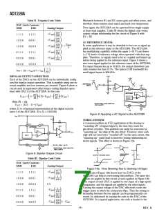
Figure 13. Variation of VREF with Feedback Configuration
MICRO P RO CESSO R INTERFACING
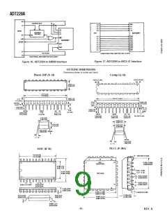
Figure 14. AD7228A to 8085A/Z80 Interface
Figure 11. Coarse/Fine Adjust Circuit
SELF-P RO GRAMMABLE REFERENCE
T he circuit of Figure 12 shows how one DAC of the AD7228,
in this case DAC1, may be used in a feedback configuration to
provide a programmable reference for itself and the other seven
converters. T he relationship of VREF to VIN is expressed by
1 + G
(
)
VREF
=
•VIN
where G = R2/R1
1 + G • D
(
)
1
Figure 13 shows typical plots of VREF versus digital code, D1, for
three different values of G. With VIN = 2.5 V and G = 3 the
voltage at the output varies between 2.5 V and 10 V giving an
effective 10-bit dynamic range to the other seven converters. For
correct operation of the circuit, VSS should be –5 V and R1
greater than 6.8 kΩ.
Figure 15. AD7228A to 6809/6502 Interface
–7–
REV. A

 ROCHESTER [ Rochester Electronics ]