AD7228A
(V = +5 V ؎ 5%, V ; = 0 to –5 V ؎ 10%, GND = 0 V, V = +1.25 V, R = 2 k⍀, C = 100 pF
DD
SS
REF
L
L
+5 V SUPPLY OPERATION
unless otherwise noted.) AII specifications TMIN to TMAX unless otherwise noted.
B
C
T
U
P aram eter
Version
Version
Version
Version
Units
Conditions/Com m ents
ST AT IC PERFORMANCE
Resolution
8
8
8
8
Bits
Relative Accuracy
Differential Nonlinearity
Full-Scale Error
Zero Code Error
@ 25°C
±2
±1
±4
±2
±1
±2
±2
±1
±4
±2
±1
±2
LSB max
LSB max
LSB max
Guaranteed Monotonic
±30
±40
±20
±30
±30
±40
±20
±30
mV max
mV max
T MIN to T MAX
REFERENCE INPUT
Reference Input Range
1.2
1.3
2
1.2
1.3
2
1.2
1.3
2
1.2
1.3
2
V min
V max
kΩ min
pF max
Reference Input Resistance
Reference Input Capacitance
500
500
500
500
POWER REQUIREMENT S
Positive Supply Range
Positive Supply Current
@ 25°C
4.75/5.25
4.75/5.25
4.75/5.25
4.75/5.25
V min/V max
For Specified Performance
16
20
16
20
16
22
16
22
µA max
µA max
T MIN to T MAX
Negative Supply Current
@ 25°C
T MIN to T MAX
14
18
14
18
14
20
14
20
µA max
µA max
NOT ES
All of the specifications as per Dual Supply Specifications except for negative full-scale settling-time when VSS = 0 V.
Specifications subject to change without notice.
1, 2
SWITCHING CHARACTERISTICS
(See Figures 1, 2; V = +5 V ؎ 5% or +10.8 V to +16.5 V; V = 0 V or –5 V ؎ 10%)
DD
SS
Lim it at 25°C
Lim it at TMIN, TMAX
(B, C Versions)
Lim it at TMIN, TMAX
(T, U Versions)
P aram eters
All Grades
Units
Conditions/Com m ents
t1
t2
t3
t4
t5
0
0
70
10
95
0
0
90
10
120
0
0
100
10
ns min
ns min
ns min
ns min
ns min
Address to WR Setup T ime
Address to WR Hold T ime
Data Valid to WR Setup T ime
Data Valid to WR Hold T ime
Write Pulse Width
150
NOT ES
1Sample tested at 25°C to ensure compliance. All input rise and fall times measured from 10% to 90% of +5 V, tR = tF = 5 ns.
VINH +VINL
2T iming measurement reference level is
2
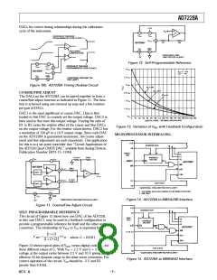
INTERFACE LO GIC INFO RMATIO N
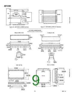
Address lines A0, A1 and A2 select which DAC accepts data
from the input port. T able I shows the selection table for the
eight DACs with Figure 1 showing the input control logic.
When the WR signal is low, the input latch of the selected DAC
is transparent, and its output responds to activity on the data
bus. T he data is latched into the addressed DAC latch on the
rising edge of WR. While WR is high, the analog outputs remain
at the value corresponding to the data held in their respective
latches.
Table I. AD 7228A Truth Table
AD 7228A Control Inputs
AD 7228A
O peration
Figure 1. Input Control Logic
WR
A2
A1
A0
H
X
X
X
No Operation
Device Not Selected
DAC 1 T ransparent
DAC 1 Latched
DAC 2 T ransparent
DAC 3 T ransparent
DAC 4 T ransparent
DAC 5 T ransparent
DAC 6 T ransparent
DAC 7 T ransparent
DAC 8 T ransparent
L
g
L
L
L
L
L
L
L
L
L
L
L
L
H
H
H
H
L
L
L
H
H
L
L
H
H
L
L
H
L
H
L
H
L
H
H = High State L = Low State X = Don’t Care
Figure 2. Write Cycle Tim ing Diagram
–3–
REV. A

 ROCHESTER [ Rochester Electronics ]