AD7228A
Table II. Unipolar Code Table
Mismatch between R1 and R2 causes gain and offset errors, and
therefore, these resistors must match and track over temperature.
D AC Latch Contents
Once again, the AD7228A can be operated from single supply
or from dual supplies. T able III shows the digital code versus
output voltage relationship for the circuit of Figure 8 with
R1 = R2.
MSB
LSB
Analog O utput
255
+VREF
1 1 1 1
1 0 0 0
1 0 0 0
0 1 1 1
0 0 0 0
0 0 0 0
1 1 1 1
0 0 0 1
0 0 0 0
1 1 1 1
0 0 0 1
0 0 0 0
256
129
256
+VREF
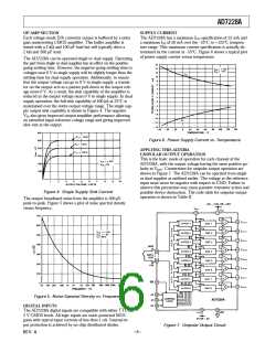
AC REFERENCE SIGNAL
VREF
2
128
In some applications it may be desirable to have an ac signal ap-
plied as the reference input to the AD7228A. T he AD7228A
has multiplying capability within the upper (+10 V) and lower
(+2 V) limits of reference voltage when operated with dual sup-
plies. T herefore, ac signals need to be ac coupled and biased up
before being applied to the reference input. Figure 9 shows a
sine-wave signal applied to the reference input of the AD7228A.
For input frequencies up to 50 kHz, the output distortion typi-
cally remains less than 0.1%. T he typical 3 dB bandwidth for
small signal inputs is 800 kHz.
+VREF
+VREF
+VREF
= +
256
127
256
1
256
0 V
1
Note: 1 LSB = (VREF)(2–8) = VREF
256
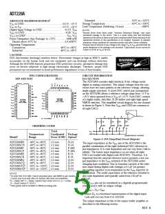
BIP O LAR O UTP UT O P ERATIO N
Each of the DACs on the AD7228A can be individually config-
ured for bipolar output operation. T his is possible using one ex-
ternal amplifier and two resistors per channel. Figure 8 shows a
circuit used to implement offset binary coding (bipolar opera-
tion) with DAC1 of the AD7228A. In this case
R2
R1
R2
R1
VOUT = 1 +
• D •V
–
• V
(
REF
(
)
)
1
REF
With R1 = R2
VOUT = (2D1 – 1) • (VREF
)
where D1 is a fractional representation of the digital word in
latch 1 of the AD7228A. (0 ≤ D1 ≤ 255/256)
Figure 9. Applying a AC Signal to the AD7228A
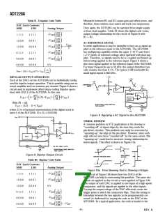
TIMING D ESKEW
A common problem in AT E applications is the slowing or
“rounding-off” of signal edges by the time they reach the
pin-driver circuitry. T his problem can easily be overcome by
“squaring-up” the edge at the pin-driver. However, since each
edge will not have been “rounded-off” by the same extent, this
“squaring-up” could lead to incorrect timing relationship be-
tween signals. T his effect is shown in Figure 10a.
Figure 8. Bipolar Output Circuit
Table III. Bipolar Code Table
D AC Latch Contents
MSB
LSB
Analog O utput
Figure 10a. Tim e Skewing Due to Slowing of Edges
127
+VREF
1 1 1 1
1 0 0 0
1 0 0 0
0 1 1 1
0 0 0 0
0 0 0 0
1 1 1 1
0 0 0 1
0 0 0 0
1 1 1 1
0 0 0 1
0 0 0 0
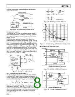
T he circuit of Figure 10b shows how two DACs of the
128
AD7228A can help in overcoming this problem. T he same two
signals are applied to this circuit as were applied in Figure 10b.
T he output of each DAC is applied to one input of a high-speed
comparator, and the signals are applied to the other inputs.
Varying the output voltage of the DAC effectively varies the
trigger point at which the comparator flips. T hus the timing re-
lationship between the two signals can be programmably cor-
rected (or deskewed) by varying the code to the DAC of the
AD7228A. In a typical application, the code is loaded to the
1
128
+VREF
0 V
1
–VREF
128
127
128
128
128
–VREF
–VREF
= –VREF
–6–
REV. A

 ROCHESTER [ Rochester Electronics ]