AD7228A
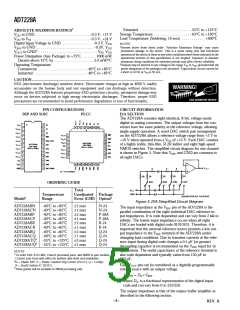
ABSO LUTE MAXIMUM RATINGS1
Extended . . . . . . . . . . . . . . . . . . . . . . . . . –55°C to +125°C
Storage T emperature . . . . . . . . . . . . . . . . . . –65°C to +150°C
Lead T emperature (Soldering, 10 secs) . . . . . . . . . . . +300°C
VDD to GND . . . . . . . . . . . . . . . . . . . . . . . . . . . –0.3 V, +17 V
VDD to VSS . . . . . . . . . . . . . . . . . . . . . . . . . . . . . –0.3 V, +24 V
Digital Input Voltage to GND . . . . . . . . . . . . . . . –0.3 V, VDD
VREF to GND . . . . . . . . . . . . . . . . . . . . . . . . . . . . . –0.3V, VDD
VOUT to GND2 . . . . . . . . . . . . . . . . . . . . . . . . . . . . . . VSS, VDD
Power Dissipation (Any Package) to +75°C . . . . . . . 1000 mW
Derates above 75°C by . . . . . . . . . . . . . . . . . . . . 2.0 mW/°C
Operating T emperature
NOT ES
1Stresses above those listed under “Absolute Maximum Ratings” may cause
permanent damage to the device. T his is a stress rating only and functional
operation of the device at these or any other conditions above those indicated in the
operational sections of this specification is not implied. Exposure to absolute
maximum rating conditions for extended periods may affect device reliability.
2Outputs may be shorted to any voltage in the range VSS to VDD provided that the
power dissipation of the package is not exceeded. T ypical short circuit current for
a short to GND or VSS is 50 mA.
Commercial . . . . . . . . . . . . . . . . . . . . . . . . –40°C to +85°C
Industrial . . . . . . . . . . . . . . . . . . . . . . . . . . –40°C to +85°C
CAUTIO N
ESD (electrostatic discharge) sensitive device. Electrostatic charges as high as 4000 V readily
accumulate on the human body and test equipment and can discharge without detection.
Although the AD7228A features proprietary ESD protection circuitry, permanent damage may
occur on devices subjected to high energy electrostatic discharges. T herefore, proper ESD
precautions are recommended to avoid performance degradation or loss of functionality.
WARNING!
ESD SENSITIVE DEVICE
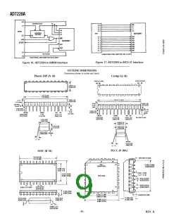
P IN CO NFIGURATIO NS
D IP AND SO IC P LCC
CIRCUIT INFO RMATIO N
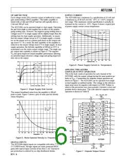
D /A SECTIO N
T he AD7228A contains eight identical, 8-bit, voltage-mode
digital-to-analog converters. T he output voltages from the con-
verters have the same polarity as the reference voltage, allowing
single supply operation. A novel DAC switch pair arrangement
on the AD7228A allows a reference voltage range from +2 V to
+10 V when operated from a VDD of +15 V. Each DAC consists
of a highly stable, thin-film, R-2R ladder and eight high-speed
NMOS switches. T he simplified circuit diagram for one channel
is shown in Figure 3. Note that VREF and GND are common to
all eight DACs.
O RD ERING GUID E
Total
Unadjusted
Error (LSB) O ption2
Tem perature
Range
P ackage
Model1
Figure 3. D/A Sim plified Circuit Diagram
AD7228ABN
AD7228ACN
AD7228ABP
AD7228ACP
AD7228ABR
AD7228ACR
AD7228ABQ
AD7228ACQ
AD7228AT Q3
–40°C to +85°C
–40°C to +85°C
–40°C to +85°C
–40°C to +85°C
–40°C to +85°C
–40°C to +85°C
–40°C to +85°C
–40°C to +85°C
–55°C to +125°C
±2 max
±1 max
±2 max
±1 max
±2 max
±1 max
±2 max
±1 max
±2 max
±1 max
N-24
N-24
P-28A
P-28A
R-24
R-24
Q-24
Q-24
Q-24
Q-24
T he input impedance at the VREF pin of the AD7228A is the
parallel combination of the eight individual DAC reference in-
put impedances. It is code dependent and can vary from 2 kΩ to
infinity. T he lowest input impedance occurs when all eight
DACs are loaded with digital code 01010101. T herefore, it is
important that the external reference source presents a low out-
put impedance to the VREF terminal of the AD7228A under
changing load conditions. Due to transient currents at the refer-
ence input during digital code changes a 0.1 µF (or greater)
decoupling capacitor is recommended on the VREF input for dc
applications. T he nodal capacitance at the reference terminal is
also code dependent and typically varies from 120 pF to
350 pF.
AD7228AUQ3 –55°C to +125°C
NOT ES
1T o order MIL-ST D-883, Class B processed parts, add /883B to part number.
Contact your local sales office for military data sheet and availability.
2N = Plastic DIP; P = Plastic Leaded Chip Carrier (PLCC); Q = Cerdip;
R = Small Outline IC (SOIC).
Each VOUT pin can be considered as a digitally programmable
voltage source with an output voltage:
3T hese grades will be available to /883B processing only.
VOUTN = DN • VREF
where DN is a fractional representation of the digital input
code and can vary from 0 to 255/256.
T he output impedance is that of the output buffer amplifier as
described in the following section.
–4–
REV. A

 ROCHESTER [ Rochester Electronics ]