The AD7245A/AD7248A is an enhanced version of the industry standard AD7245/AD7248. Improvements include operation from 12 V to 15 V supplies,
a ±1/2 LSB linearity grade, faster interface times and better full scale and reference variations with VDD. Additional features include extended
temperature range operation for commercial and industrial grades.
The AD7245A/AD7248A is a complete, 12-bit, voltage output, digital-to-analog converter with output amplifier and Zener voltage reference on a
monolithic CMOS chip. No external user trims are required to achieve full specified performance.
Both parts are microprocessor compatible, with high speed data latches and double-buffered interface logic. The AD7245A accepts 12-bit parallel data
which is loaded into the input latch on the rising edge of CS or WR. The AD7248A has an 8-bit wide data bus with data loaded to the input latch in two
write operations. For both parts, an asynchronous LDAC signal transfers data from the input latch to the DAC latch and updates the analog output. The
AD7245A also has a CLR signal on the DAC latch which allows features such as power-on reset to be implemented.
The on-chip 5 V buried Zener diode provides a low noise, temperature compensated reference for the DAC. For single supply operation, two output
ranges of 0 V to +5 V and 0 V to +10 V are available, while these two ranges plus an additional ±5 V range are available with dual supplies. The output
amplifiers are capable of developing +10 V across a 2 kOhm load to GND.
2
The AD7245A/AD7248A is fabricated in linear compatible CMOS (LC MOS), an advanced, mixed technology process that combines precision bipolar
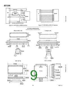
circuits with low power CMOS logic. The AD7245A is available in a small, 0.3" wide, 24-pin DIP and SOIC and in 28-terminal surface mount packages.
The AD7248A is packaged in a small, 0.3" wide, 20-pin DIP SOIC and in 20-terminal surface mount packages.

 ROCHESTER [ Rochester Electronics ]