RT9214
Under Voltage Protection
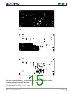
placement layout and printed circuit design can minimize
the voltage spikes induced in the converter. Consider, as
an example, the turn-off transition of the upper MOSFET
prior to turn-off, the upper MOSFET was carrying the full
load current. During turn-off, current stops flowing in the
upper MOSFET and is picked up by the low side MOSFET
or schottky diode. Any inductance in the switched current
path generates a large voltage spike during the switching
interval. Careful component selections, layout of the
critical components, and use shorter and wider PCB traces
help in minimizing the magnitude of voltage spikes.
The voltage at FB pin is monitored and protected against
UV (under voltage). The UV threshold is the FB or FBL
under 80%. UV detection has 15μs triggered delay. When
OC is trigged, a hiccup restart sequence will be initialized,
as shown in Figure 7 Only 4 times of trigger are allowed
to latch off. Hiccup is disabled during soft-start interval,
but UV_FB has some difference from OC, it will always
trigger VIN power sensing after 4 times hiccup, as shown
in Figure 8.
COUNT = 1
COUNT = 2
COUNT = 3
COUNT = 4
There are two sets of critical components in a DC-DC
converter using the RT9214. The switching power
components are most critical because they switch large
amounts of energy, and as such, they tend to generate
equally large amounts of noise. The critical small signal
components are those connected to sensitive nodes or
those supplying critical bypass current.
4V
2V
0V
OVERLOAD
APPLIED
0A
T0
T1
T2
T3
T4
The power components and the PWM controller should
be placed firstly. Place the input capacitors, especially
the high-frequency ceramic decoupling capacitors, close
to the power switches. Place the output inductor and
output capacitors between the MOSFETs and the load.
Also locate the PWM controller near by MOSFETs.
TIME
Figure 7. UV and OC trigger hiccup mode
Power Off
A multi-layer printed circuit board is recommended.
UGATE
FB
(20V/Div)
Figure 9 shows the connections of the critical components
in the converter. Note that the capacitors CIN and COUT
each of them represents numerous physical capacitors.
Use a dedicated grounding plane and use vias to ground
all critical components to this layer. Apply another solid
layer as a power plane and cut this plane into smaller
islands of common voltage levels. The power plane should
support the input power and output power nodes. Use
copper filled polygons on the top and bottom circuit layers
for the PHASE node, but it is not necessary to oversize
this particular island. Since the PHASE node is subjected
to very high dV/dt voltages, the stray capacitance formed
between these island and the surrounding circuitry will
tend to couple switching noise. Use the remaining printed
circuit layers for small signal routing. The PCB traces
between the PWM controller and the gate of MOSFET
and also the traces connecting source of MOSFETs should
be sized to carry 2A peak currents.
UV
VIN Power
Sensing
(500mV/Div)
VOUT
VIN
(2V/Div)
(2V/Div)
IOUT = 2A
Time (10ms/Div)
Figure 8, UV_FB trigger VIN power sensing
PWM Layout Considerations
MOSFETs switch very fast and efficiently. The speed with
which the current transitions from one device to another
causes voltage spikes across the interconnecting
impedances and parasitic circuit elements. The voltage
spikes can degrade efficiency and radiate noise, that results
in over-voltage stress on devices. Careful component
www.richtek.com
13
DS9214-13 September 2007

 RICHTEK [ RICHTEK TECHNOLOGY CORPORATION ]