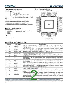
RT8876A
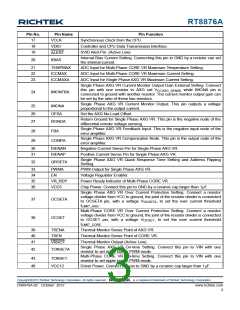
Pin No.
Pin Name
Pin Function
49, 53, 47
50, 54, 46
LGATE [1:3]
PHASE [1:3]
Low Side Drive Output. This pin drives the gate of low side MOSFET.
Switch node of High Side Driver. Connect the pin to high side MOSFET source
together with the low side MOSFET drain and the inductor.
51, 55, 45
52, 56, 44
UGATE [1:3]
BOOT [1:3]
High Side Drive Output. Connect the pin to the gate of high side MOSFET.
Bootstrap Power Pin. This pin powers high side MOSFET driver.
57
Ground. The exposed pad must be soldered to a large PCB and connected to
GND for maximum power dissipation.
GND
(Exposed Pad)
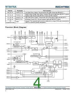
Function Block Diagram
Current
Monitor
Current
Monitor
Offset
Generator
IMON
MUX
ADC
POR
UVLO
V
SETA
V
SET
GND
From Control Logic
DAC
Control &
Protection Logic
QRSET
RGNDA
SVID XCVR
QRSETA
V
SETA
Soft-Start & Slew
Rate Control
ERROR
AMP
PWM
CMP
+/-
+
-
TON
Gen
+
-
PWMA
FBA
COMPA
DVIDA
Offset
Cancellation
TONSETA
1/20
To Protection Logic
OVP/UVP/NVP
DVID
1/20
From Control Logic
Offset
ISENAP
ISENAN
+
OCP
20
-
OFS
Generator
DAC
OCSETA
TONSET
RGND
PWM
CMP
Soft-Start & Slew
Rate Control
V
SET
+
-
+
-
BOOTx
FB
Offset
Cancellation
UGATEx
PHASEx
LGATEx
TON
Gen
3-PH
Driver
COMP
QR
CMP
+
PWM
[1:3]
+
-
PHASE
Selector
V
QR_TRIP
IBIAS
RSET
ISEN3P
ISEN3N
+
10
-
To Protection Logic
OVP/UVP/NVP OCP
Current Balance
SUM
ISEN2P
ISEN2N
+
10
-
ISEN1P
ISEN1N
+
10
-
OCSET
Copyright 2012 Richtek Technology Corporation. All rights reserved.
©
is a registered trademark of Richtek Technology Corporation.
www.richtek.com
4
DS8876A-02 October 2012

 RICHTEK [ RICHTEK TECHNOLOGY CORPORATION ]