RT8876A
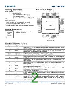
Pin Configurations
Ordering Information
RT8876A
(TOP VIEW)
Package Type
QW : WQFN-56L 7x7 (W-Type)
Lead Plating System
56 55 54 53 52 51 50 49 48 47 46 45 44 43
G : Green (Halogen Free and Pb Free)
1
2
42
41
40
39
38
37
36
35
34
33
32
31
30
29
QRSET
DVIDA
ISEN2P
ISEN2N
ISEN1N
ISEN1P
ISEN3P
ISEN3N
RSET
COMP
FB
RGND
DVID
TONSETA
VRHOT
TSEN
TSENA
OCSET
OCSETA
VCC5
VR_RDY
EN
PWMA
Note :
3
Richtek products are :
4
` RoHS compliant and compatible with the current
requirements of IPC/JEDEC J-STD-020.
` Suitable for use in SnPb or Pb-free soldering processes.
5
6
7
GND
8
9
10
11
12
13
14
57
QRSETA
ISENAP
ISENAN
COMPA
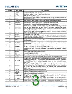
Marking Information
RT8876AGQW : Product Number
OFS
RT8876A
GQW
YMDNN : Date Code
15 16 17 18 19 20 21 22 23 24 25 26 27 28
YMDNN
WQFN-56L 7x7
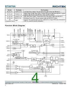
Functional Pin Description
Pin No.
Pin Name
Pin Function
Multi-phase CORE VR channel quick response time setting and initial voltage
(V ) setting.
1
QRSET
INITIAL
Place a resistor and a capacitor from this pin to GND to enhance DVID
performance. Short this pin to GND if not use.
2
DVIDA
5, 4, 8
6, 3, 7
ISEN [1:3] N
ISEN [1:3] P
Negative Current Sense Pin of Phase 1, 2, 3 for CORE VR.
Positive Current Sense Pin of Phase 1, 2, 3 for CORE VR.
Multi-Phase CORE VR Ramp Setting. This is used to set the multi-phase
CORE VR loop external ramp slope.
9
RSET
COMP
FB
Multi-Phase CORE VR Compensation Node. This pin is the output node of the
error amplifier.
10
11
12
Multi-Phase CORE VR Feedback Input. This is the negative input node of the
error amplifier.
Return Ground for Multi-Phase CORE VR. This pin is the negative node of the
differential remote voltage sensing.
RGND
Place a Resistor and a Capacitor from this Pin to GND to enhance DVID
Performance. Short this pin to GND if not use.
13
14
15
DVID
OFS
Output Voltage Offset Setting.
Current Monitor Output. This pin outputs a voltage proportional to the output
current.
IMON
Current Monitor Output Gain External Setting. Connect this pin with one
resistor to CPU V
while IMON pin is connected to ground with one
CC_SENSE
16
IMONFB
another resistor. The current monitor output gain can be set by the ratio of
these two resistors.
Copyright 2012 Richtek Technology Corporation. All rights reserved.
©
is a registered trademark of Richtek Technology Corporation.
www.richtek.com
2
DS8876A-02 October 2012

 RICHTEK [ RICHTEK TECHNOLOGY CORPORATION ]