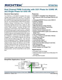
RT8876A
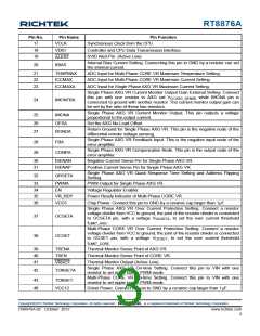
Pin No.
17
Pin Name
VCLK
Pin Function
Synchronous Clock from the CPU.
18
VDIO
Controller and CPU Data Transmission Interface.
SVID Alert Pin. (Active Low)
19
ALERT
Internal Bias Current Setting. Connecting this pin to GND by a resistor can set
the internal current.
20
IBIAS
21
22
23
TEMPMAX
ICCMAX
ADC Input for Multi-Phase CORE VR Maximum Temperature Setting.
ADC Input for Multi-Phase CORE VR Maximum Current Setting.
ADC Input for Single Phase AXG VR Maximum Current Setting.
Single Phase AXG VR Current Monitor Output Gain External Setting. Connect
ICCMAXA
this pin with one resistor to AXG rail V
connected to ground with another resistor. The current monitor output gain can
be set by the ratio of these two resistors.
while IMONA pin is
CCAXG_SENSE
24
IMONFBA
Single Phase AXG VR Current Monitor Output. This pin outputs a voltage
proportional to the output current.
25
26
27
IMONA
OFSA
Set the AXG No-Load Offset.
Return Ground for Single Phase AXG VR. This pin is the negative node of the
differential remote voltage sensing.
RGNDA
Single Phase AXG VR Feedback Input. This is the negative input node of the
error amplifier.
28
29
FBA
Single Phase AXG VR Compensation Node. This pin is the output node of the
error amplifier.
COMPA
30
31
ISENAN
ISENAP
Negative Current Sense Pin for Single Phase AXG VR.
Positive Current Sense Pin for Single Phase AXG VR.
Single Phase AXG VR Quick Response Time Setting and Address Flipping
Setting.
32
QRSETA
33
34
35
36
PWMA
EN
PWM Output for Single Phase AXG VR.
Voltage Regulator Enabler.
VR_RDY
VCC5
Power Ready Indicator of Multi-Phase CORE VR.
Chip Power. Connect this pin to GND by a ceramic cap larger than 1μF.
Single Phase AXG VR Over Current Protection Setting. Connect a resistor
voltage divider from VCC to ground, the joint of the resistor divider is connected
37
38
OCSETA
OCSET
to OCSETA pin, with a voltage V
, to set the over current threshold
OCSETA
I
.
LIMIT_AXG
Multi-Phase CORE VR Over Current Protection Setting. Connect a resistor
voltage divider from VCC to ground, the joint of the resistor divider is connected
to OCSET pin, with a voltage V
, to set the over current threshold
OCSET
I
.
LIMIT_CORE
39
40
41
TSENA
TSEN
Thermal Monitor Sense Point of AXG VR.
Thermal Monitor Sense Point of CORE VR.
Thermal Monitor Output (Active Low).
VRHOT
Single Phase AXG VR On-time Setting. Connect this pin to VIN with one
resistor to set ripple size in PWM-mode.
42
TONSETA
Multi-Phase CORE VR On-time Setting. Connect this pin to VIN with one
resistor to set ripple size in PWM-mode.
43
48
TONSET
VCC12
Driver Power. Connect this pin to GND by a ceramic cap larger than 1μF.
Copyright 2012 Richtek Technology Corporation. All rights reserved.
©
is a registered trademark of Richtek Technology Corporation.
DS8876A-02 October 2012
www.richtek.com
3

 RICHTEK [ RICHTEK TECHNOLOGY CORPORATION ]