RT8859M
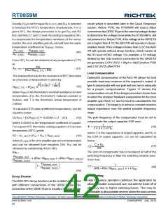
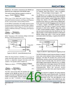
IMONA pin. The resistor connected to the IMONA pin
determines the voltage gain of the IMONA output.
designers should design VIMONA to be 3.3V at ICCMAXA.
For example, when load current = 50% x ICCMAXA,
VIMONA = 1.65V and Output_Current register = 7Fh.
The current monitor indicator equation is shown as :
I
x R
R
x R
LOAD
DROOP IMONA
The IMONA pin is an output of the internal operational
amplifier and sends out IMONA signal. When the data of
Output_Current register reaches 255d (when IMONA
voltage rises above 3.3V), the ALERT signal will be
asserted to low, which is so-called SVID ICCMAXA alert.
In the mean time, the AXGVR will assert the bit 2 data to
1 in Status_1 register. The ALERT assertion will be de-
asserted when the data of Output_Current register
decreases to 242d (when IMONA voltage falls under
3.144V). The bit 2 assertion of Status_1 register is latched
and can only be cleared when two criteria are met : the
data of Output_Current register decreases to 242d (when
IMONA voltage falls under 3.144V) and the GetReg
command is sent to the Status_1 register of theAXGVR.
(58)
V
=
IMONA
IMONFBA
Where ILOAD is the output load current, RDROOP is the
equivalent load line resistance, and RIMONA and RIMONFBA
are the current monitor current setting resistors.
In VR12/IMVP7 specification, the voltage signal of current
monitoring will be restricted by a maximum value. Platform
designers have to select RIMONA to meet the maximum
voltage of IMONA at full load. Find RIMONA and RIMONFBA
based on :
V
RIMONA
IMONA(MAX)
=
(59)
RIMONFBA IMAX x RDROOP
where VIMONA(MAX) is the maximum voltage at full load,
and IMAX is the full load current of VR.
Quick Response
Current Mirror
Current Mirror
V
FBA
+ 2(V
)
ISENA
V
+
-
V
DAC, AXG
OLL EN
CCAXG_SENSE
+
QR trigger
I
V
CCAXG_SENSE
-
R
IMONFBA
IMONFBA
V
FBA
R
Mirror
IMONFBA
IMONFBA
IMONA
I
Mirror
R
IMONA
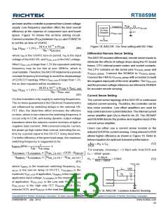
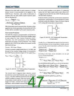
Figure 23. AXGVR : Quick Response Triggering Circuit
Figure 22. AXGVR : Current Monitoring Circuit
The AXGVR utilizes a quick response feature to support
heavy load current demand during instantaneous load
transient. The AXG VR monitors the current of the
IMONFBApin, and this current is mirrored to internal quick
response circuit. At steady state, this mirrored current
will not trigger a quick response. When the VOUT,AXG voltage
drops abruptly due to load apply transient, the mirrored
current into quick response circuit will also increase
instantaneously. When the mirrored current
instantaneously rises above 5μA, quick response will be
triggered.
When the droop function is disabled, VCCAXG_SENSE no
longer varies with output current, so the current monitoring
function is adaptively changed internally under this
situation. The equation will be rewritten as :
2 x I
x R
x R
IMONA
LOAD
RDCR
V
=
IMONA, NO_DROOP
R
IMONFBA
(60)
(61)
V
RIMONA
IMONA(MAX)
=
RIMONFBA 2 x IMAX x RDCR
The ADC circuit of the AXG VR monitors the voltage
variation at the IMONA pin from 0V to 3.3V, and this
voltage is decoded into digital format and stored into the
Output_Current register. The ADC divides 3.3V into 255
levels, so LSB = 3.3V/255 = 12.941mV. Platform
When quick response is triggered, the quick response
circuit will generate a quick response pulse. The internal
quick response pulse generation circuit is similar to the
on-time generation circuit. The only difference is the
QRSETA pin. The voltage at the QRSETA pin also
Copyright 2012 Richtek Technology Corporation. All rights reserved.
©
is a registered trademark of Richtek Technology Corporation.
www.richtek.com
46
DS8859M-05 July 2012

 RICHTEK [ RICHTEK TECHNOLOGY CORPORATION ]