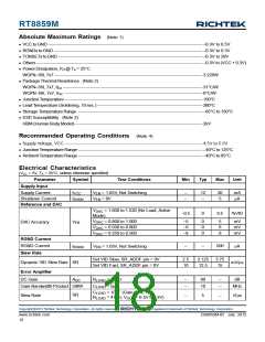
RT8859M
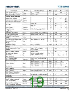
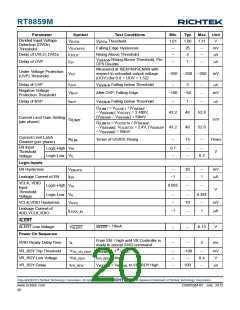
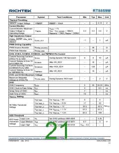
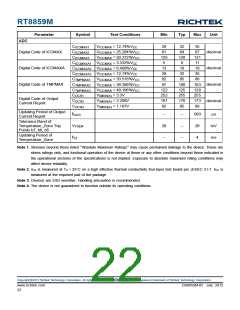
Parameter
ADC
Symbol
Test Conditions
Min
Typ
Max
Unit
C
C
C
C
C
C
C
C
C
C
C
C
V
V
V
V
V
V
V
V
V
V
V
V
= 12.74%V
CC
29
61
32
64
35
67
ICCMAX1
ICCMAX2
ICCMAX3
ICCMAXA1
ICCMAXA2
ICCMAXA3
TMPMAX1
TMPMAX2
TMPMAX3
OCR1
ICCMAX
ICCMAX
ICCMAX
ICCMAX
ICCMAX
ICCMAX
ICCMAX
ICCMAX
ICCMAX
IMON(A)
IMON(A)
IMON(A)
Digital Code of ICCMAX
Digital Code of ICCMAXA
Digital Code of TMPMAX
= 25.284%V
= 50.372%V
decimal
decimal
decimal
decimal
CC
CC
125
5
128
8
131
11
= 3.332%V
= 6.468%V
= 12.74%V
CC
13
16
19
CC
CC
29
32
35
= 33.516%V
= 39.396%V
= 49.196%V
= 3.3V
82
85
88
CC
CC
CC
97
100
125
255
170
85
103
128
255
173
88
122
252
167
82
Digital Code of Output
Current Report
= 2.208V
OCR2
= 1.107V
OCR3
Updating Period of Output
Current Report
tOCR
--
20
--
--
--
--
500
20
4
μs
mV
ms
Tolerance Band of
Temperature_Zone Trip
Points b7, b6, b5
V
TSEN
Updating Period of
Temperature_Zone
tTZ
Note 1. Stresses beyond those listed “Absolute Maximum Ratings” may cause permanent damage to the device. These are
stress ratings only, and functional operation of the device at these or any other conditions beyond those indicated in
the operational sections of the specifications is not implied. Exposure to absolute maximum rating conditions may
affect device reliability.
Note 2. θJA is measured at TA = 25°C on a high effective thermal conductivity four-layer test board per JEDEC 51-7. θJC is
measured at the exposed pad of the package.
Note 3. Devices are ESD sensitive. Handling precaution is recommended.
Note 4. The device is not guaranteed to function outside its operating conditions.
Copyright 2012 Richtek Technology Corporation. All rights reserved.
©
is a registered trademark of Richtek Technology Corporation.
www.richtek.com
22
DS8859M-05 July 2012

 RICHTEK [ RICHTEK TECHNOLOGY CORPORATION ]