RT8859M
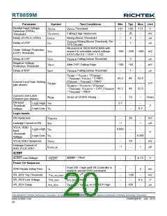
Parameter
Symbol
Test Conditions
Min
Typ
Max
Unit
Thermal Throttling
--
--
0.13
V
VRHOT Output Voltage
VVRHOT
IVRHOT = 10mA
Current Monitor
Current Monitor Maximum
Output Voltage in
Operating Range
VDAC = 1V,
VFB − VCC_SENSE = 100mV,
RIMONFB = 10kΩ, RIMON = 330kΩ
VIMON
3.2
3.3
--
3.4
1
V
High Impedance Output
PWMx, ALERT, VRx_RDY,
VRHOT
ILEAK_OUT
−1
μA
PWM Driving Capability
PWM Source Resistor
PWM Sink Resistor
RPWM_SOURCE
RPWM_SINK
--
--
30
15
--
--
Ω
Ω
DVID, DVIDA, ICCMAX, ICCMAXA, and TMPMAX Pin Current
Current Sourcing Out from
DVIDx Pin to GND
IDVIDx
During dynamic VID fast event
6
--
--
--
8
10
--
μA
μA
μA
μA
Current Sinking In from 5V
to ICCMAX Pin
Current Sourcing Out from
ICCMAXA Pin to GND
Current Sinking In from 5V
to TMPMAX Pin
IICCMAX
IICCMAXA
ITMPMAX
After VR_RDY
After VRA_RDY
After VR_RDY
16
128
16
--
--
DVID and DVIDA Maximum Voltage
Maximum Allowable
Voltage at DVIDx Pin
VDVIDx_MAX
During Dynamic VID Event
--
--
2
V
SVID
SVID Frequency
fSVID
5
4
25
--
26.25 MHz
SVID Clock to Data Delay tCO
8.3
--
ns
ns
ns
Setup Time of VDIO
Hold Time of VDIO
VINITIAL Setting
tSU
tHLD
7
--
14
--
--
VSETINI0
For VINITIAL = 0V
0
--
8
VSETINI0_9
VSETINI1_0
VSETINI1_1
VSETINI1_5
For VINITIAL = 0.9V
For VINITIAL = 1V
For VINITIAL = 1.1V
For VINITIAL = 1.5V
17
--
--
--
--
20
SETINIx Threshold
Voltage
%VCC
32.5
57.5
82.5
42.5
67.5
100
ADD Threshold
Logic-Low
VIL
Set SVID address 0000 0001
Set SVID address 0010 0011
Set SVID address 0100 0101
--
0.7
--
--
--
0.35
3
ADD Input
Threshold
Voltage
V
Logic-Medium VIM
Logic-High VIH
VCC − 0.2
--
Copyright 2012 Richtek Technology Corporation. All rights reserved.
©
is a registered trademark of Richtek Technology Corporation.
DS8859M-05 July 2012
www.richtek.com
21

 RICHTEK [ RICHTEK TECHNOLOGY CORPORATION ]