RT8859M
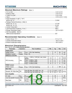
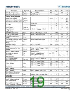
Parameter
Symbol
VCOMP
IOUTEA
Test Conditions
RLOAD = 47kΩ
Min
Typ
Max
Unit
Output Voltage Range
MAX Source/Sink Current
Current Sense Amplifier
Input Offset Voltage
0.3
--
--
3.6
--
V
VCOMP = 2V
250
μA
VOSCS
−0.75
1
--
--
0.75
--
mV
MΩ
MΩ
Impedance at Negative Input RISENxN
Impedance at Positive Input RISENxP
1
--
--
CORE VR
AXG VR
--
10
20
--
--
DC Gain
V/V
--
--
Input Range
VISEN_IN
−50
−1
100
1
mV
%
VISEN Linearity
VISEN_ACC
−30mV < VISEN_IN < 50mV
--
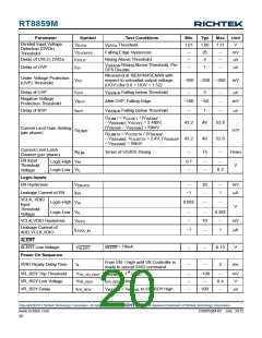
tON Setting
TONSETx Pin Voltage
CCM On-Time Setting
VTON
tON
IRTON = 80μA, VDAC = 0.75V
IRTON = 80μA, PS0, PS1
--
1.07
305
--
V
275
335
ns
TONSETx Input Current
Range
IRTON
25
--
280
μA
On-Time in PS2 (Core only) tON_PS2
With Respect to PS0 tON
--
--
85
--
--
%
Minimum Off-Time
IBIAS
tOFF
250
ns
IBIAS Pin Voltage
QRSET
VIBIAS
RIBIAS = 53.6kΩ
2.09
2.14
2.19
V
Quick Response On-Time
Setting
VDAC = 0.75V, VQRSET = 1.2V,
tONx_QR
--
305
--
ns
I
RTON = 80μA
QRSET Source Current
IQRSET
VIH
Before UVLO
--
VCC − 0.5
--
80
--
--
--
μA
V
No Load Line Setting
Threshold
QRSET Voltage before
UVLO, Relative to VCC
VIL
--
VCC − 1.8
V
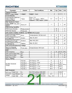
OFS Function
OFS Enable/Disable
Threshold Voltage
VOFS > VEN_OFS before EN
rising
VEN_OFS
0.7
1.2
--
V
1.62
0.69
0.9
1
VID = 1V, VOFS = 1.83V
VID = 1V, VOFS = 0.9V
VID = 1V, VOFS = 1.2V
1.63
0.7
1
1.64
0.71
1.01
--
Offset Voltage
VOUT
ROFS
VRSET
V
MΩ
V
Impedance
--
RSET Setting
RSET Voltage
RSET Voltage, VDAC = 1V
0.97
--
1
1
1.03
--
Zero Current Detection
Zero Current Detection
Threshold
VZCD
ISEN1P (AP) − ISEN1N (AN)
mV
Protection
Falling Edge, 100mV
Hysteresis
VUVLO
4.04
--
4.24
100
150
4.44
--
V
Under Voltage Lock-out
(UVLO)Threshold
ΔVUVLO
VOVABS
Falling Edge Hysteresis
mV
mV
Absolute Over Voltage
(OVP) Protection Threshold
With respect to VOUT_Max
100
200
Copyright 2012 Richtek Technology Corporation. All rights reserved.
©
is a registered trademark of Richtek Technology Corporation.
DS8859M-05 July 2012
www.richtek.com
19

 RICHTEK [ RICHTEK TECHNOLOGY CORPORATION ]